InGaAs/AlGaAs single quantum well and multi-quantum well semiconductor laser active region epitaxial structure
A multi-quantum well structure and multi-quantum well technology, which is applied in the field of semiconductor materials, can solve the problem of small GaAs band gap and achieve the effects of enhanced luminous intensity, enhanced photoluminescence intensity, and small FWHM
- Summary
- Abstract
- Description
- Claims
- Application Information
AI Technical Summary
Problems solved by technology
Method used
Image

Examples
Embodiment 1
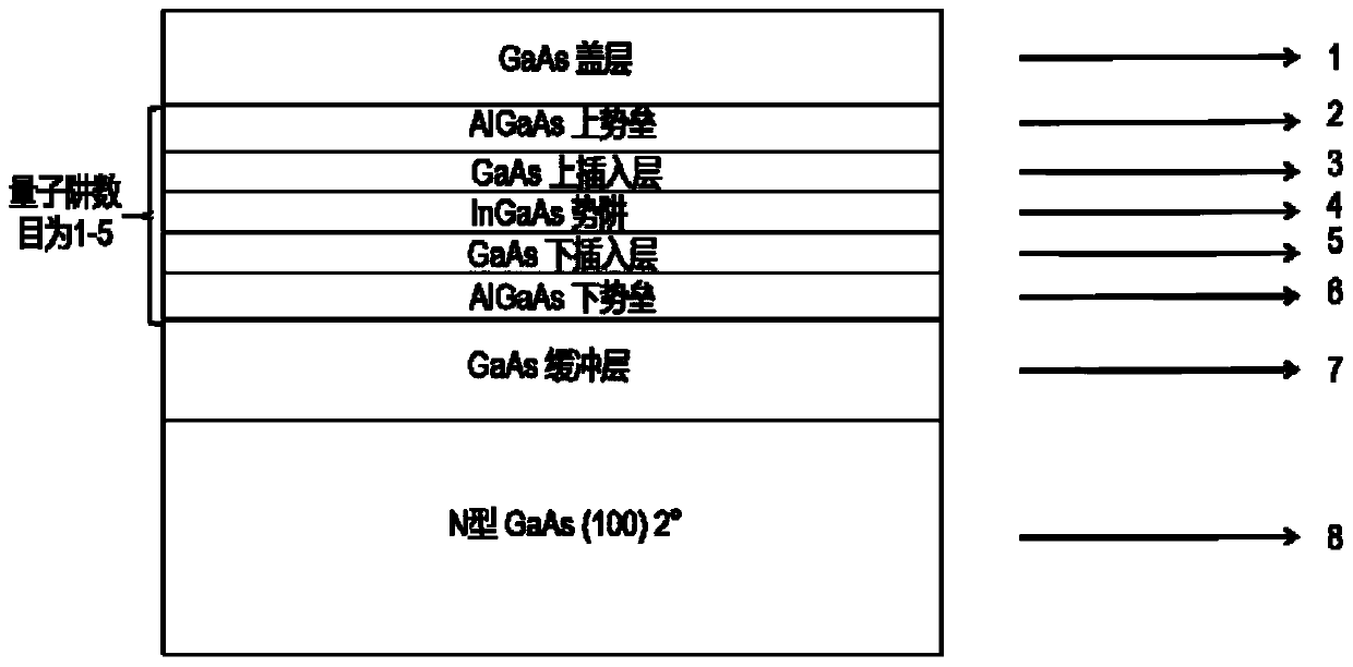
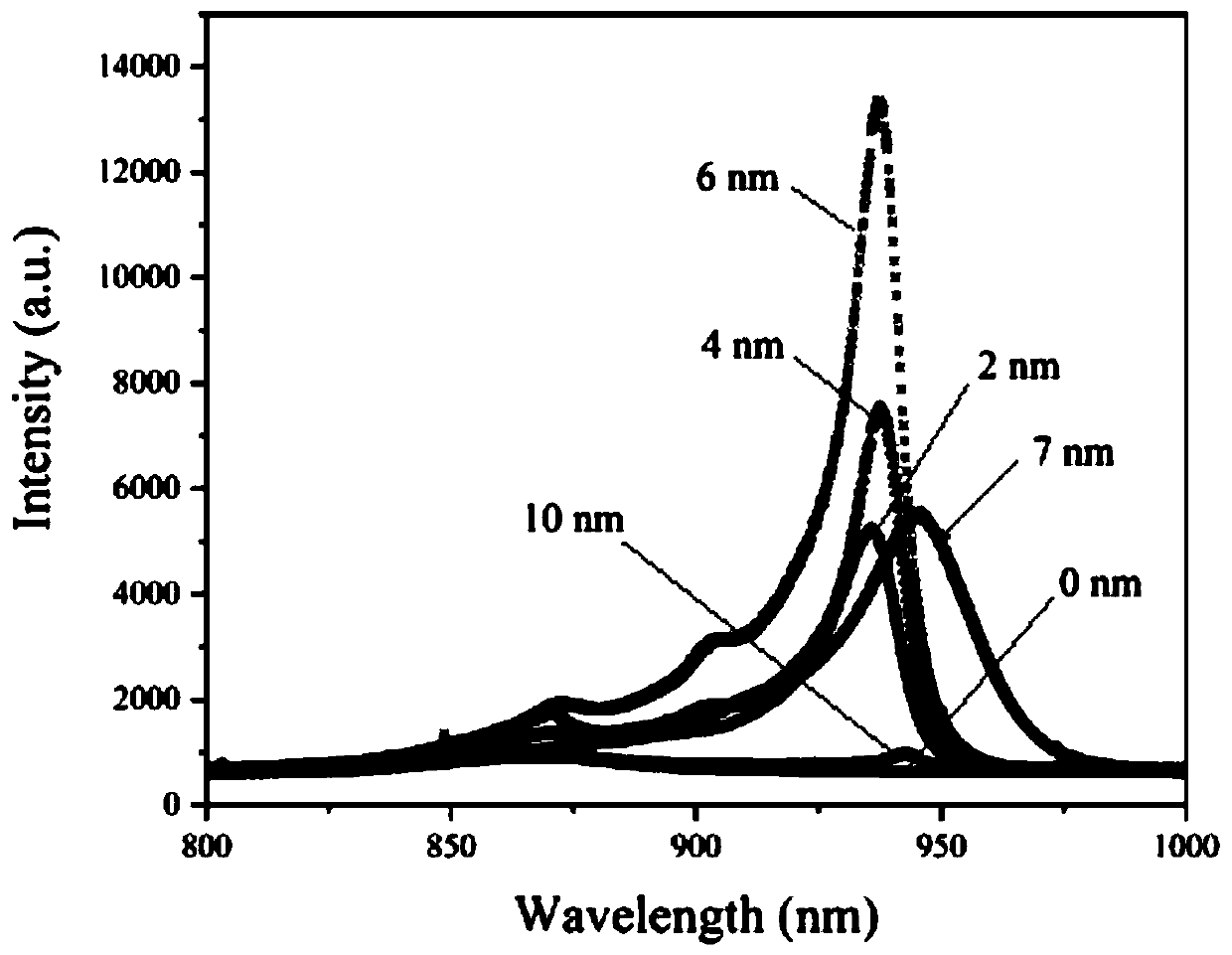
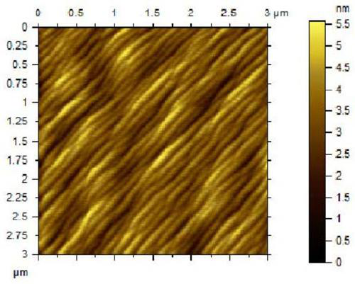
[0032] In this embodiment, the structure of the active region of the semiconductor laser is obtained by epitaxy using MOCVD technology, in which the upper barrier layer 2 of AlGaAs and the lower barrier layer 6 of AlGaAs are both Al 0.3 GaAs, 680°C high temperature growth; InGaAs potential well layer 4 is In 0.18 GaAs is grown at a low temperature of 600°C; the GaAs upper insertion layer 3 and the GaAs lower insertion layer 5 are 0nm respectively, and the upper and lower insertion layers are grown at a low temperature of 600°C and a high temperature of 680°C, respectively. In order to characterize the luminous efficiency and crystal quality of the active region of the multi-quantum well structure, the epitaxial wafer was tested by photoluminescence and atomic force microscopy. Such as figure 2 As shown, it is a photoluminescence spectrum diagram, and the luminous intensity is almost 0 (relative intensity). Such as image 3 As shown, it is the surface topography map of atom...
Embodiment 2
[0034] In this embodiment, the structure of the active region of the semiconductor laser is obtained by epitaxy using MOCVD technology, in which the upper barrier layer 2 of AlGaAs and the lower barrier layer 6 of AlGaAs are both Al 0.3 GaAs, 680°C high temperature growth; InGaAs potential well layer 4 is In 0.18 GaAs is grown at a low temperature of 600°C; the GaAs upper insertion layer 3 and the GaAs lower insertion layer 5 are 4nm, and the upper and lower insertion layers are grown at a low temperature of 600°C and a high temperature of 680°C, respectively. In order to characterize the luminous efficiency and crystal quality of the active region of the multi-quantum well structure, the epitaxial wafer was tested by photoluminescence and atomic force microscopy. Such as figure 2 As shown, it is a photoluminescence spectrum diagram, the luminous intensity is 7544 (relative intensity), the half-maximum width is 16.5nm, and the lasing wavelength is 937nm. Such as Figure 4 ...
Embodiment 3
[0036] In this embodiment, the structure of the active region of the semiconductor laser is obtained by epitaxy using MOCVD technology, in which the upper barrier layer 2 of AlGaAs and the lower barrier layer 6 of AlGaAs are both Al 0.3 GaAs, 680°C high temperature growth; InGaAs potential well layer 4 is In 0.18GaAs is grown at a low temperature of 600°C; the GaAs upper insertion layer 3 and the GaAs lower insertion layer 5 are 6nm, and the upper and lower insertion layers are grown at a low temperature of 600°C and a high temperature of 680°C, respectively. In order to characterize the luminous efficiency and crystal quality of the active region of the multi-quantum well structure, the epitaxial wafer was tested by photoluminescence and atomic force microscopy. Such as figure 2 As shown, it is a photoluminescence spectrum diagram, the luminous intensity is 13361 (relative intensity), the half-maximum width is 14.5nm, and the lasing wavelength is 937nm. Such as Figure 5 ...
PUM
| Property | Measurement | Unit |
|---|---|---|
| Surface roughness | aaaaa | aaaaa |
| Half width | aaaaa | aaaaa |
| Half width | aaaaa | aaaaa |
Abstract
Description
Claims
Application Information
PatSnap Eureka turns technology decisions into work you can execute. Powered by our Innovation Knowledge Graph, it runs expert workflows across engineering, life sciences, materials and intellectual property. Get your review-ready output in minutes.


