fet and method of forming fet

A semiconductor and crystal technology, used in semiconductor devices, electrical components, circuits, etc., to solve problems such as reduced device performance and high leakage current of FinFETs

Active Publication Date: 2019-07-19
TAIWAN SEMICON MFG CO LTD
View PDF4 Cites 0 Cited by
  • Summary
  • Abstract
  • Description
  • Claims
  • Application Information

AI Technical Summary

Problems solved by technology

[0003] However, there are challenges in the realization of such components and processes in semiconductor manufacturing
For example, poor isolation between adjacent fins results in high leakage current for FinFETs, thereby degrading device performance

Method used


Image

  • fet and method of forming fet
  • fet and method of forming fet
  • fet and method of forming fet

Examples


Embodiment

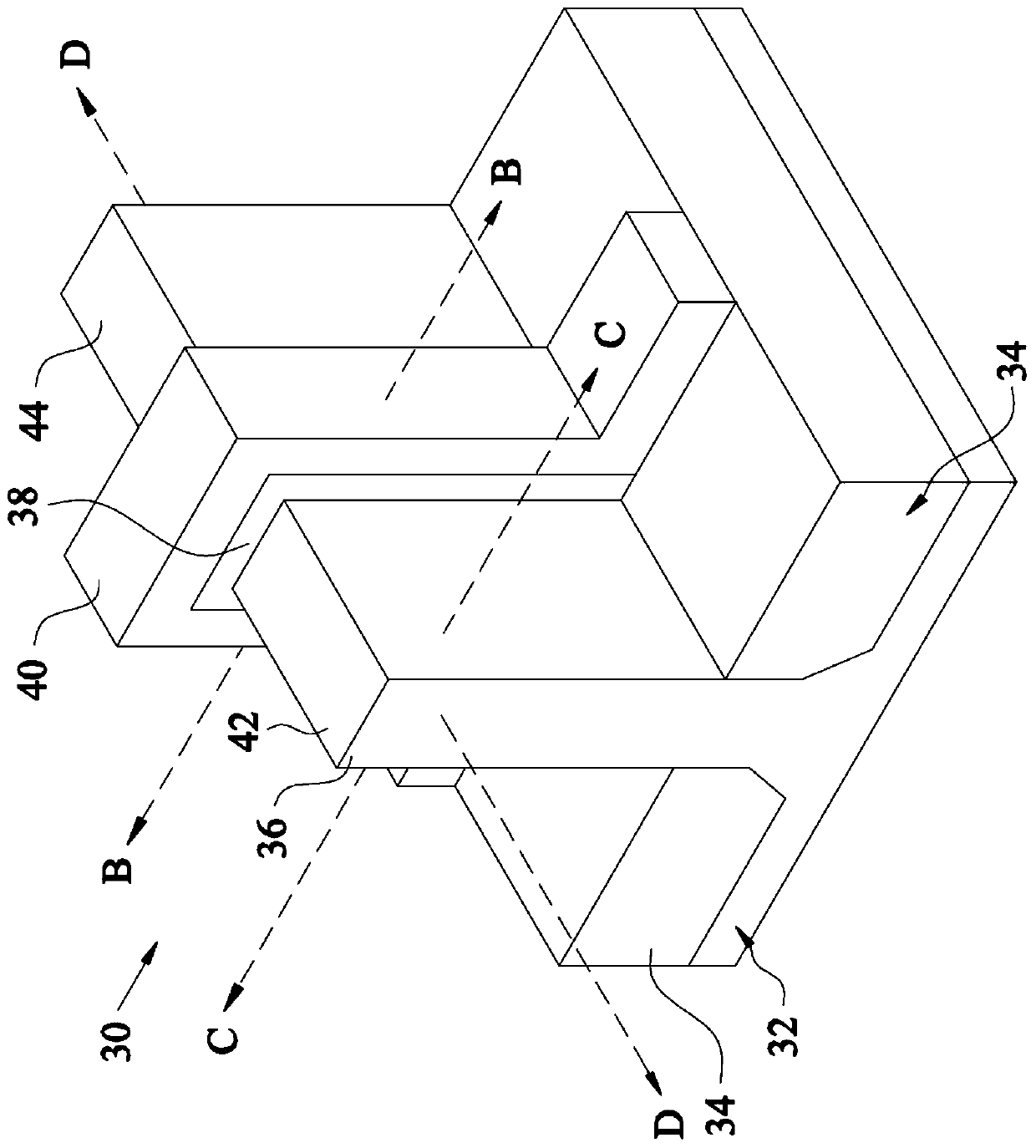
[0070] An embodiment is a method comprising forming a first fin and a second fin on a substrate, the first fin and the second fin each comprising a first crystalline semiconductor material on the substrate and a first fin over the first crystalline semiconductor material The second crystalline semiconductor material. The first crystalline semiconductor material in the second fin is converted to a dielectric material, wherein at least a portion of the first crystalline semiconductor material in the first fin remains untransformed after the converting step. A gate structure is formed over the first fin and the second fin, and source / drain regions are formed on opposite sides of the gate structure.

[0071] Another embodiment is a method comprising epitaxially growing a first crystalline semiconductor material on a substrate, epitaxially growing a second crystalline semiconductor material over the first crystalline semiconductor material, and patterning the first crystalline semi...


PUM

PropertyMeasurementUnit
thicknessaaaaaaaaaa
thicknessaaaaaaaaaa

Abstract

An embodiment is a method including forming a first fin and a second fin on a substrate, the first fin and the second fin each including a first crystalline semiconductor material on a substrate and a second crystalline semiconductor material above the first crystalline semiconductor material. Converting the first crystalline semiconductor material in the second fin to a dielectric material, wherein after the converting step, at least a portion of the first crystalline semiconductor material in the first fin remains unconverted. Forming gate structures over the first fin and the second fin, and forming source / drain regions on opposing sides of the gate structures.

Description

technical field [0001] Embodiments of the invention relate to FETs and methods of forming FETs. Background technique [0002] In the pursuit of higher device density, higher performance, and lower cost, as semiconductor devices have advanced to nanotechnology process nodes, challenges from fabrication and design issues have led to the development of three-dimensional devices, such as fin field-effect transistors ( FinFETs). Typical FinFETs are fabricated with thin vertical "fins" (or fin structures) extending from a substrate formed by, for example, etching away a portion of the silicon layer of the substrate. In this vertical fin the channel of the FinFET is formed. A gate is provided over (eg, surrounding) the fin. Having gates on both sides of the channel allows gate control of the channel from both sides. [0003] A challenge, however, is the implementation of such components and processes in semiconductor manufacturing. For example, poor isolation between adjacent ...

Claims


Application Information

Patent Timeline
Patent Type & Authority Patents(China)
IPC IPC(8): H01L21/336H01L29/78
CPCH01L27/0924H01L21/02236H01L21/02255H01L21/823821H01L21/823878H01L29/0642H01L29/165
Inventor 江国诚刘继文王志豪
Owner TAIWAN SEMICON MFG CO LTD
Why Eureka
Try Eureka