Flip chip packaging structure and packaging method

A technology of flip-chip packaging and sealant, which is applied in the direction of semiconductor/solid-state device parts, semiconductor devices, electrical components, etc., and can solve the problems of inability to effectively control the size and randomness of the overflow of the adhesive material

Active Publication Date: 2020-08-07
CHIPMORE TECH CORP LTD +1
View PDF5 Cites 0 Cited by
  • Summary
  • Abstract
  • Description
  • Claims
  • Application Information

AI Technical Summary

Problems solved by technology

[0004] In the prior art, when coating the adhesive material around the chip, the randomness is large, and the size of the adhesive material overflow cannot be effectively controlled after the adhesive material is coated in the dispensing process.

Method used


Image

  • Flip chip packaging structure and packaging method
  • Flip chip packaging structure and packaging method
  • Flip chip packaging structure and packaging method

Examples


Embodiment Construction

[0027] The embodiments described below by referring to the figures are exemplary only for explaining the present invention and should not be construed as limiting the present invention.

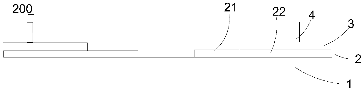
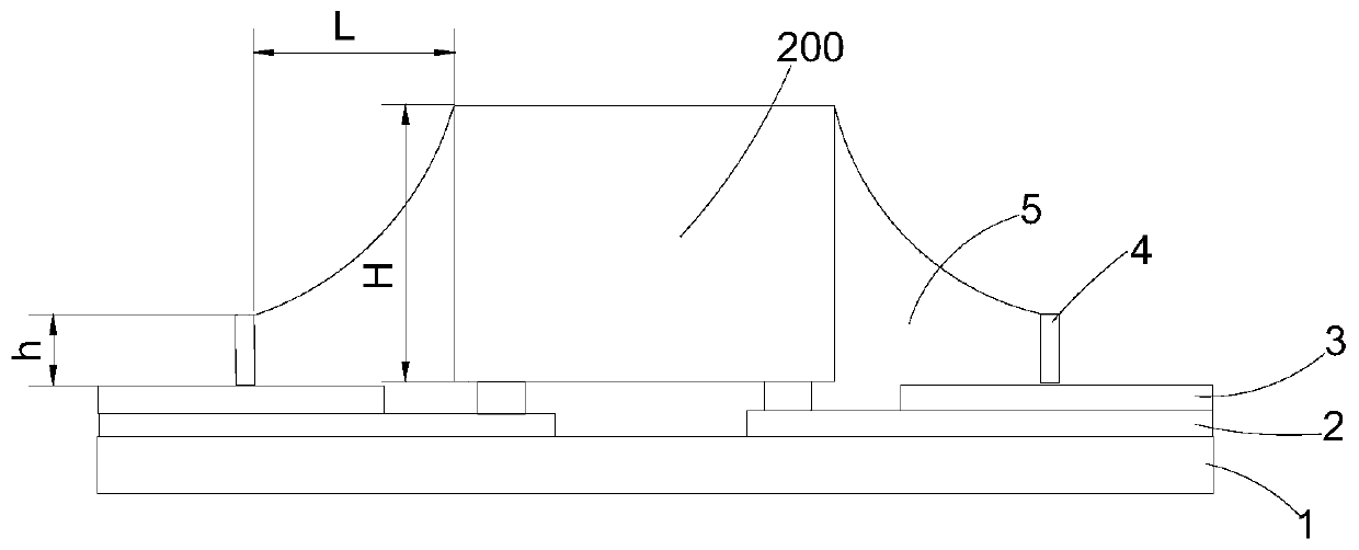
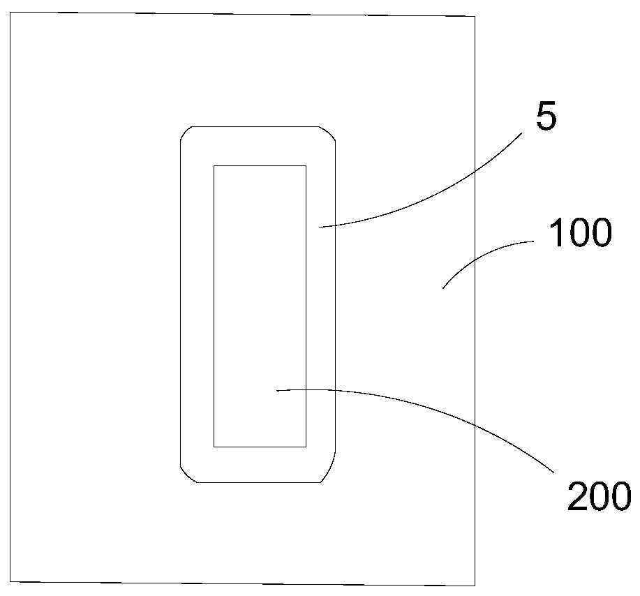
[0028] Embodiments of the present invention: as Figure 1-3 As shown, a flexible circuit board is disclosed, including a base layer 1, a circuit layer 2 and a protective layer 3 arranged on the surface of the base layer 1, and the circuit layer 2 has an internal connection area 21 for connecting with a flip chip 200 and the coverage area 22 covered by said protective layer 3 . The flexible circuit board also has a barrier 4 disposed on the protective layer 3 and protruding in a direction away from the protective layer 3 .

[0029] The covering area 22 is covered by the protection layer 3 to protect the wiring thereon, and the inner connection area 21 is exposed without being covered by the protection layer 3 for connection and fixation with the pins of the flip chip 200 . The middle positio...


PUM


Abstract

The invention discloses a flip chip packaging structure and a packaging method. The flip chip packaging structure comprises a flexible circuit board and a flip chip installed on the flexible circuit board. The flexible circuit board comprises a base layer, a circuit layer and a protective layer, wherein the circuit layer and the protective layer are arranged on the surface of the base layer; the side, provided with a flip chip, of the flexible circuit board is provided with a blocking body which is arranged on the protective layer and protrudes in the direction away from the protective layer;a sealant layer is arranged between the blocking body and the flip chip; the height h of the blocking body is not less than H-L; L represents the distance from the blocking body to the flip chip; H represents the vertical distance between the top of the sealant layer and the protective layer. The flow of the sealant is limited between the blocking body and the flip chip through the arrangement ofthe blocking body, so that the width of the sealant layer on the protective layer is effectively controlled, and the overflow of the sealant layer is effectively controlled.

Description

technical field [0001] The invention relates to the technical field of electronic manufacturing, in particular to a flip-chip packaging structure and packaging method. Background technique [0002] With the rapid development of the electronics industry, products with flip-chip packaging structures have the advantages of small size, high performance, and short leads, which also makes flip-chip packaging technology increasingly become the mainstream technology in the industry. During the preparation process of the flexible circuit board for flip-chip packaging, in order to protect the circuit on the flexible circuit board and avoid short circuit caused by foreign objects falling, scratching or oxidation; Prepare a layer of protective film on the surface of the circuit that does not need to be soldered, while the circuit that requires subsequent soldering does not need to prepare a protective film. In the actual production process, a layer of solder resist paint is generally a...

Claims


Application Information

Patent Timeline
Patent Type & Authority Applications(China)
IPC IPC(8): H01L23/31H01L23/498H01L21/56
CPCH01L23/3185H01L23/49838H01L21/56H01L2224/16225H01L2224/73204H01L2224/32225H01L2224/26175H01L2924/00
Inventor 石浩
Owner CHIPMORE TECH CORP LTD
Why Eureka
Try Eureka