Automatic ICT test device

A test device and automatic technology, applied in the direction of measuring device, electronic circuit test, measuring electricity, etc., can solve the problems of low automation, achieve high automation, reduce time cost, and ensure reliability

Active Publication Date: 2020-08-18
西安精雕软件科技有限公司
16 Cites 0 Cited by

AI-Extracted Technical Summary

Problems solved by technology

[0004] The object of the present invention is to provide an automatic ICT test device to solve the problem in...

Method used

As shown in Figures 1 and 2, the lifting mechanism 1 is fixed with the mechanism frame 2 by the leveling plate 18, and the leveling screw 15 is housed between the leveling plate 18 and the fixture mounting plate 17, and its effect is to adjust the height of the lifting mechanism 1 Make it parallel to the circuit board 43 to be tested on the circuit board fixture 4, the leveling screw 15 passes through the threaded hole on the fixture mounting plate 17, and the lower end pushes against the leveling plate 18, and adjusts the position of the leveling screw 15 The relative positions of the leveling plate 18 and the jig mounting plate 17 can be changed to achieve the purpose of leveling. The nut 16 is used to lock the leveling screw 16 after leveling so that the lifting mechanism 1 maintains the current posture, and after locking, the leveling plate 18 and the jig mounting plate 17 are fixed together with screws. The cylinder 11 is installed on the jig mounting plate 17 , and the cylinder rod is connected with the pressing plate 19 . The linear bearing 14 is installed on the jig mounting plate 17 , and the guide shaft 12 passes through the linear bearing 14 and is connected with the pressure plate 19 . When the cylinder 11 moves, it drives the pressure plate 19 to move up and down, and is guided by the guide shaft 12 to improve the positioning accuracy of the test probe 36 . The collar 13 is fixed on the linear bearing 14 and its position can be adjusted, which is used to adjust the stroke of the lifting mechanism 1 to adapt to the height of the circuit board jig 4 .
[0042] The two bosses on both sides of the probe tray 31 are used to connect with the two connection blocks 110 on the lifting mechanism 1. There are V-shaped grooves in the middle part of the outer side of the boss, which are used to clamp the ball plunger 111 in the middle part of the connecting block 110, so as to realize the rough positioning of the probe tra...

Abstract

The invention provides an automatic ICT test device, which comprises a lifting mechanism, a mechanism frame and a probe jig. The lifting mechanism is installed on the mechanism frame, and the probe jig is installed on the lifting mechanism. The probe jig is installed on the lifting mechanism, accurate positioning is achieved through the positioning pins, and different PCBs can be quickly replaced.A plurality of probes communicated with the ICT test instrument are installed in the probe jig, and the probes are distributed in one-to-one correspondence with the positions of test points on the PCB. And a positioning column is mounted on the probe jig and is used for accurately positioning the PCB circuit board jig. An air cylinder on the lifting mechanism can drive the probe jig to automatically ascend or descend, and when the probe jig ascends, the probe jig can be replaced; and when the probe jig descends, the probe is in contact with the measuring point, so that testing and program programming of the ICT test instrument on the PCB are realized.

Application Domain

Electronic circuit testingElectrical measurement instrument details

Technology Topic

Tester deviceInstrumentation +3

Image

  • Automatic ICT test device
  • Automatic ICT test device
  • Automatic ICT test device

Examples

  • Experimental program(1)
  • Effect test(1)

Example Embodiment

[0035] The following detailed descriptions are all exemplary descriptions and are intended to provide further detailed descriptions of the present invention. Unless otherwise specified, all technical terms used in the present invention have the same meanings as commonly understood by those skilled in the art to which this application belongs. The terms used in the present invention are only for describing specific embodiments, and are not intended to limit the exemplary embodiments according to the present invention.
[0036] The embodiment of the present invention is an automatic ICT test device.
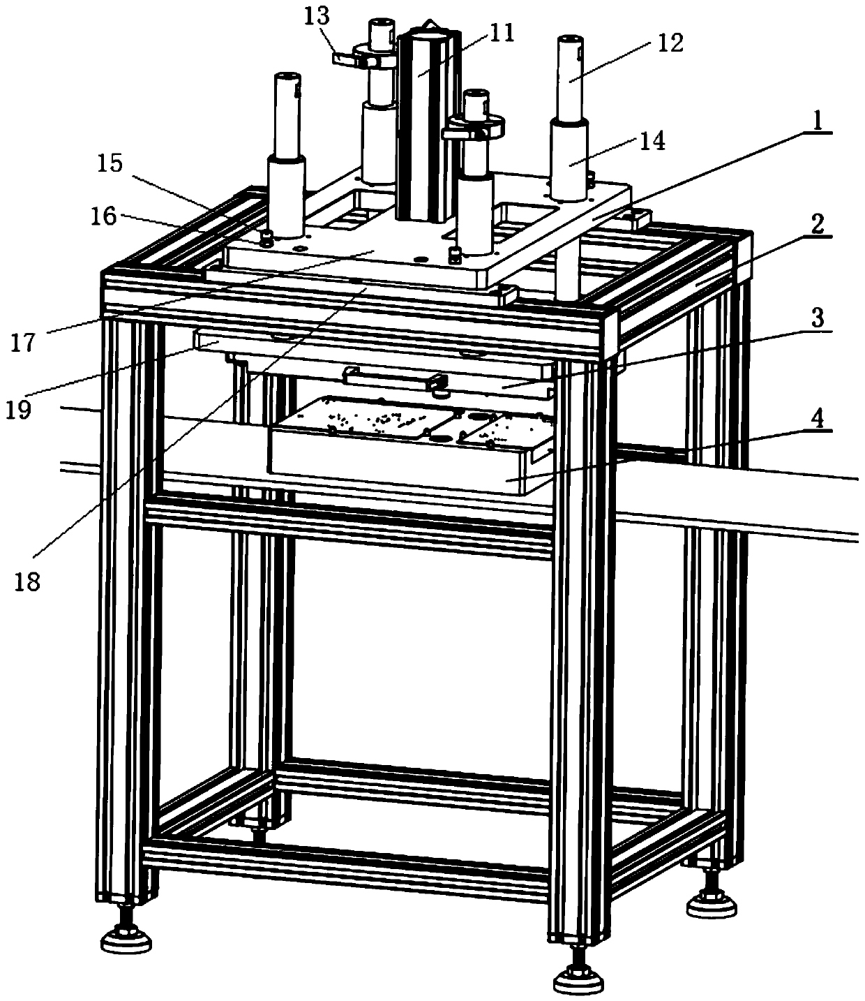
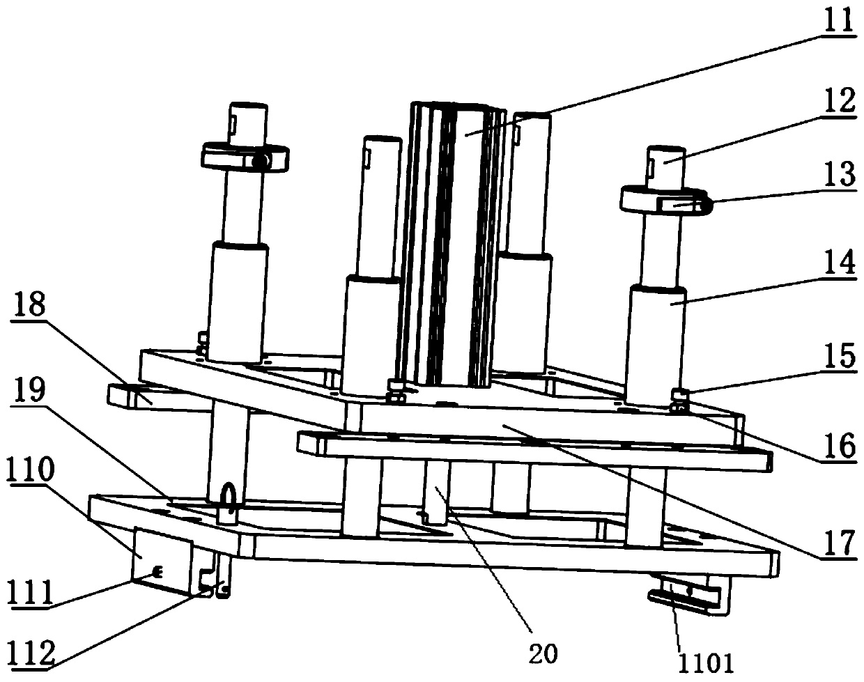
[0037] Principle description: The lifting mechanism 1 is integrally installed on the mechanism frame 2, and its function is to drive the probe jig 3 to raise and lower. When raised, the probe fixture can be replaced and the circuit board fixture 4 can be placed, transported, adjusted and other operations; when lowered, push the probe tray 31 down to make the probe 36 on the probe tray and the test The corresponding test points on the circuit board 43 are in contact with each other to realize the detection and programming of the circuit board 43 to be tested.
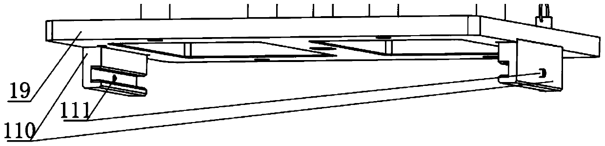
[0038] Such as figure 1 with 2 As shown, the lifting mechanism 1 is fixed to the mechanism frame 2 by a leveling plate 18, and a leveling screw 15 is installed between the leveling plate 18 and the fixture mounting plate 17, and its function is to adjust the level of the lifting mechanism 1 to the circuit board fixture. The circuit board 43 to be tested on 4 is kept parallel, the leveling screw 15 passes through the threaded hole on the fixture mounting plate 17, and the lower end is topped on the leveling plate 18. Adjusting the position of the leveling screw 15 can change the leveling plate 18 and the fixture The relative position of the mounting plate 17 is used for leveling purposes. The nut 16 is used to lock the leveling screw 16 to maintain the current posture of the lifting mechanism 1 after leveling, and fix the leveling plate 18 and the fixture mounting plate 17 together with screws after locking. The cylinder 11 is installed on the fixture mounting plate 17, and the cylinder rod is connected with the pressure plate 19. The linear bearing 14 is installed on the jig mounting plate 17, and the guide shaft 12 passes through the linear bearing 14 and is connected to the pressure plate 19. When the air cylinder 11 moves, the pressure plate 19 is driven to move up and down, and is guided by the guide shaft 12 to improve the positioning accuracy of the test probe 36. The collar 13 is fixed on the linear bearing 14 with an adjustable position, and is used to adjust the stroke of the lifting mechanism 1 to adapt to the height of the circuit board fixture 4.
[0039] Such as image 3 As shown, connecting blocks 110 are respectively installed on both sides under the pressure plate 19 for the purpose of placing the probe tray 31. The connecting block 110 has a rectangular chute, and the width of the rectangular chute is slightly larger than the thickness of the boss on the probe tray 31. It is convenient to insert the probe tray 31 from the side. The connecting block 110 is equipped with a ball plunger 111 for cooperating with the V-shaped grooves on both sides of the probe tray 31 to realize the rough positioning of the probe tray 31 on the lifting mechanism 1. The positioning pin 112 sequentially passes through the pin hole on the pressure plate 19 and the pin sleeve 35 on the probe tray 31, and is used for precise secondary positioning of the probe fixture 3 after being installed on the lifting mechanism 1.
[0040] Mechanism frame 2: The mechanism frame 2 is placed on the ground and used to install the lifting mechanism 1. Its composition can be profile, square steel or other structural forms.
[0041] Probe fixture 3: The probe fixture 3 is installed on the lifting mechanism 1 as a carrier of the probe 36 to assist it in performing the ICT test of the circuit board 43 to be tested. The feature of the probe fixture 3 in this patent is that it can be designed and quickly replaced for multiple/multi-type circuit boards 43 to be tested.
[0042] The two bosses on both sides of the probe tray 31 are used to connect with the two connecting blocks 110 on the lifting mechanism 1. V-shaped grooves are respectively opened in the middle of the outer side of the boss to clamp the ball plunger 111 in the middle of the connecting block 110 to realize the rough positioning of the probe tray 31. The two pin sleeves 35 are located on the probe tray 31 at diagonal angles. The line distribution is used to realize the precise secondary positioning of the probe fixture 3 and the lifting mechanism 1. A test circuit board 32 is installed on the upper surface of the probe tray 31, which is fixed by a fixing block 33; the upper surface of the test circuit board 32 is reserved with a writer connector and a power supply connector, and the cable connector of the ICT test instrument can pass through the lifting mechanism The jig mounting board 17 and the pressing board 19 of 1 are connected with the test circuit board 32 to realize the probe 36 receiving or sending data to the ICT test instrument. The probe 36 is soldered on the test circuit board 32, and the position layout of the probe corresponds to the test points on the circuit board 43 to be tested one to one, and passes through the probe fixing plate 37 and protrudes from the lower surface of the probe tray 31, which is convenient for waiting. The test points on the test circuit board 43 are connected. The probe fixing plate 37 is installed on the lower surface of the probe tray 31 to assist in guiding and fixing the probe 36. Two positioning posts 38 are installed on the lower surface of the probe tray 31 and are used to cooperate with the pin sleeve 44 on the circuit board tray 41 to accurately position the circuit board tool 4 a second time. The handle 34 is installed on the side of the probe tray to facilitate manual replacement of the probe fixture 3.
[0043] Such as Figure 4 with 5 As shown, circuit board fixture 4: The circuit board fixture 4 is placed on the workbench or assembly line, and coarsely positioned before the needle bed test, so that the test point on the circuit board 43 to be tested is as close as possible to the upper probe The probes 36 on the jig 3 correspond one to one. The circuit board 43 to be tested is placed on the circuit board tray 41 with the test point facing upwards and positioned by the stop pin 42. The positioning sleeve 44 is installed on the upper surface of the circuit board tray 41 and cooperates with the positioning post 38 on the probe fixture 3 to accurately position the circuit board fixture 4 a second time.
[0044] The working process is as follows:
[0045] When the production line is switched to production, the cylinder 11 is retracted and the lifting mechanism 1 is raised;
[0046] Manually insert the probe fixture 3 corresponding to the PCB to be tested into the two connecting blocks 110 sliding grooves under the lifting mechanism 1. When the probe fixture 3 is inserted into the connecting block 110, the ball head of the ball plunger 111 installed in the middle of the two connecting blocks 110 is pushed back by the probe fixture; when the V on both sides of the probe tray 31 When the groove slides to the ball plunger 111, the ball head is pushed out under the action of the spring force and stuck in the V-shaped groove on both sides of the probe tray 31 to roughly position the probe fixture.
[0047] Manually insert the two positioning pins 112 through the pin holes on the pressure plate 19 and insert them into the positioning pin sleeve 35 of the probe tray 31 to perform precise secondary positioning of the probe fixture 3. Since step (2) has performed rough positioning of the probe jig 3 through the ball plunger 111, the secondary positioning of this step is easier to implement.
[0048] Pass the cable plug of the ICT test instrument through the fixture mounting plate 17 and the pressure plate 19, and respectively plug them into the corresponding interface of the test circuit board 32 to realize the data transmission and power supply between the probe and the ICT test instrument. At this point, the replacement of the probe fixture is complete.
[0049] Transfer the circuit board fixture 4 to the bottom of the probe fixture 3 and make coarse positioning so that the test points on the circuit board 43 to be tested correspond to the probe 36 on the upper probe fixture 3 as much as possible; the cylinder 11 extends , The probe fixture 3 is lowered, and the two positioning posts 38 on the probe fixture 3 are respectively inserted into the two positioning sleeves 44 on the circuit board tray 41 to accurately position the circuit board fixture 4; The tool 3 continues to descend until the probes 36 respectively contact the test points on the circuit board 43 to be tested.

PUM

no PUM

Description & Claims & Application Information

We can also present the details of the Description, Claims and Application information to help users get a comprehensive understanding of the technical details of the patent, such as background art, summary of invention, brief description of drawings, description of embodiments, and other original content. On the other hand, users can also determine the specific scope of protection of the technology through the list of claims; as well as understand the changes in the life cycle of the technology with the presentation of the patent timeline. Login to view more.

Similar technology patents

Distributed storage system

InactiveUS20100115078A1improve reliabilityminimize increase in management workload
Owner:SKY PERFECT JSAT CORPORATION

Dual-Dielectric MIM Capacitors for System-on-Chip Applications

ActiveUS20100213572A1reduced process step and complexityimprove reliability
Owner:TAIWAN SEMICON MFG CO LTD

Hybrid excitation E-shaped iron core axial magnetic field permanent magnet brushless motor

InactiveCN102223036AImprove reliabilityTo achieve fault-tolerant operation
Owner:SOUTHEAST UNIV

Classification and recommendation of technical efficacy words

  • Improve reliability

Organic light emitting diode display

ActiveUS20070008268A1improve reliability
Owner:LG DISPLAY CO LTD

Method and apparatus for correcting errors in memory device

ActiveUS20120151294A1improve reliability
Owner:SAMSUNG ELECTRONICS CO LTD

Multiple branch predictions

ActiveUS20050268075A1improve reliabilityfacilitate availability
Owner:ORACLE INT CORP
Why Eureka
Try Eureka