

Wafer front-end conveying system
A technology for conveying systems and wafers, which is applied in the manufacture of conveyor objects, electrical components, and semiconductor/solid-state devices. It can solve problems such as defect detection and wafer alignment, and achieve time reduction, volume reduction and improvement efficiency effect
- Summary
- Abstract
- Description
- Claims
- Application Information
AI Technical Summary
Problems solved by technology
Method used
Image

Examples
Embodiment Construction
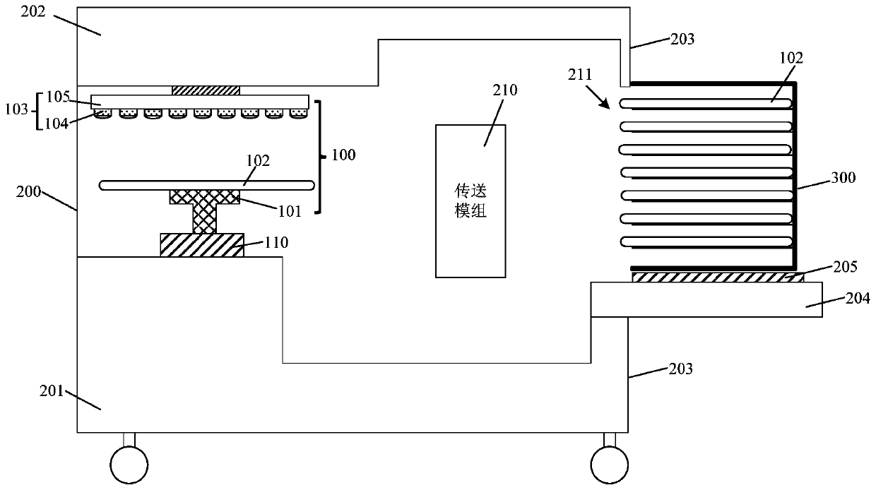
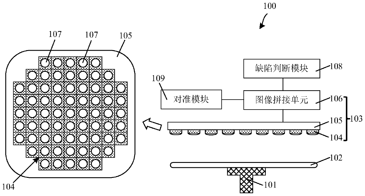
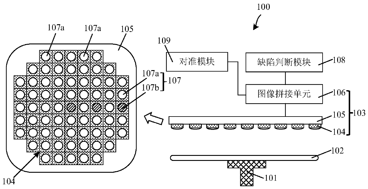
[0032] The present invention provides a wafer front-end transfer system, including: a loading platform and a defect detection module, the defect detection module is used to detect defects on the wafer and perform wafer inspection before the wafer enters the equipment end. The alignment of the circle, the defect detection module includes: a wafer carrier, used to fix the wafer that needs to be detected for defects; an image acquisition module, the image acquisition module includes a camera array, and the image acquisition module passes The first detection image corresponding to the entire surface of the wafer on the wafer carrier is obtained by one shot of the camera array or the alignment detection image corresponding to one circle of the edge of the wafer is obtained by one shot of the camera array; the defect judgment module, the defect judgment The module judges whether there is a defect on the surface of the wafer according to the first detection image obtained by the image...
PUM
 Abstract
Description
Claims
Application Information