Mini LED display panel and preparation method thereof

A technology for display panels and preparation steps, which is applied in the direction of electrical components, electric solid devices, circuits, etc., which can solve the problems of packaging difficulties, afterimages, and easy screen burn-in, and achieve the effects of reducing thickness, reducing manufacturing costs, and reducing manufacturing steps

Pending Publication Date: 2020-08-25
SHENZHEN CHINA STAR OPTOELECTRONICS SEMICON DISPLAY TECH CO LTD
View PDF4 Cites 4 Cited by
  • Summary
  • Abstract
  • Description
  • Claims
  • Application Information

AI Technical Summary

Problems solved by technology

[0004] The invention provides a mini LED display panel and a preparation method thereof, which are used to solve the technical problems of OLED products in the prior art, such as instability, difficult packaging, easy screen burn-in, and afterimages.

Method used


Image

  • Mini LED display panel and preparation method thereof
  • Mini LED display panel and preparation method thereof
  • Mini LED display panel and preparation method thereof

Examples


Embodiment 1

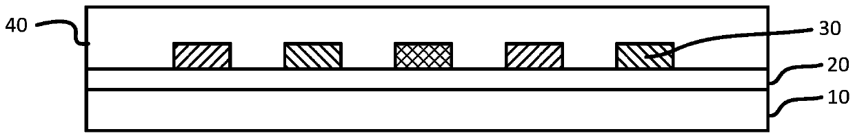
[0030] In this example, if figure 1 As shown, the mini LED display panel of the present invention includes a flexible layer 10 , a thin film transistor circuit 20 , a mini LED chip 30 and an encapsulation layer 40 .

[0031] The flexible layer 10 includes at least one of polydimethylsiloxane (PDMS, polydimethylsiloxane), polyimide film (Polyimide Film), flexible circuit board (Flexible Printed Circuit), and the flexible layer 10 has good flexibility, The mini LED display panel can be flexibly bent.

[0032] The thin film transistor circuit 20 is arranged on one side surface of the flexible layer 10. The thin film transistor circuit 20 includes several thin film transistor units, and the thin film transistor unit includes a P-type low-temperature polysilicon thin film transistor or an N-type low-temperature polysilicon thin film transistor. The thin film transistor circuit 20 includes a A plurality of scanning lines extending in the row direction, a plurality of single-ended s...

Embodiment 2

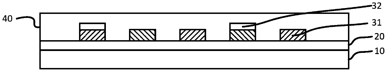
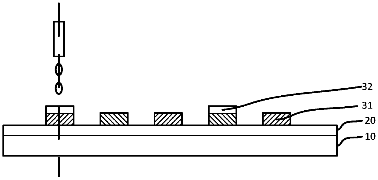
[0047] In this example, if figure 2 As shown, the mini LED display panel of the present invention includes a flexible layer 10 , a thin film transistor circuit 20 , a mini LED chip 31 and an encapsulation layer 40 .

[0048] The flexible layer 10 includes at least one of polydimethylsiloxane (PDMS, polydimethylsiloxane), polyimide film (PolyimideFilm), flexible circuit board (Flexible Printed Circuit), the flexible layer 10 has good flexibility, can The mini LED display panel realizes flexible bending.

[0049] The thin film transistor circuit 20 is arranged on one side surface of the flexible layer 10. The thin film transistor circuit 20 includes several thin film transistor units, and the thin film transistor unit includes a P-type low-temperature polysilicon thin film transistor or an N-type low-temperature polysilicon thin film transistor. The thin film transistor circuit 20 includes a A plurality of scanning lines extending in the row direction, a plurality of single-en...


PUM


Abstract

The invention discloses a mini LED display panel and a preparation method thereof. The mini LED display panel comprises a flexible layer; a thin film transistor circuit arranged on the surface of oneside of the flexible layer; and a plurality of mini led chips uniformly distributed on the surface of one side, far away from the flexible layer, of the thin film transistor circuit. The beneficial effects of the invention are that: according to the mini LED display panel and the preparation method thereof, the mini LED chips are integrated on the flexible layer, so that full-color display of themini LED display panel is realized, and the thickness of the mini LED display panel is reduced; and the transfer layer covers the mini LED chips in a transfer printing or ink-jet printing mode, so that full-color display of the mini LED display panel is achieved, meanwhile, the preparation steps of the mini LED chip can be reduced, and the preparation cost of the mini LED display panel is reduced.

Description

technical field [0001] The present application relates to the field of LEDs, in particular to a mini LED display panel and a preparation method thereof. Background technique [0002] Flexible display has become a hot focus in the display application market this year. However, the current commercial flexible display is OLED technology, but the current OLED products still have technical problems such as instability, packaging difficulties, easy screen burn-in, and afterimages. [0003] Mini-LED (miniature light-emitting diode), a new technology regarded by many manufacturers as the next-generation display, shrinks the size of the traditional LED chip to 100ˉ300um level, with power consumption much smaller than LCD (liquid crystal display), brightness better than OLED, And self-illumination and other advantages, at the same time, it has the advantages of high brightness, good luminous efficiency, light and thin, self-illumination and so on. If it is arranged in an array, it ha...

Claims


Application Information

Patent Timeline
Patent Type & Authority Applications(China)
IPC IPC(8): H01L27/15H01L27/12H01L33/48H01L33/50H01L33/62
CPCH01L27/156H01L33/48H01L33/62H01L33/502H01L27/1218H01L27/1266H01L2933/0033H01L2933/0041H01L2933/0066
Inventor 孙洋樊勇江沛柳铭岗
Owner SHENZHEN CHINA STAR OPTOELECTRONICS SEMICON DISPLAY TECH CO LTD
Why Eureka
Try Eureka