Transparent display device, simulation method and manufacturing method

A transparent display and device technology, which is applied in semiconductor/solid-state device manufacturing, electrical solid-state devices, semiconductor devices, etc., can solve problems such as pinhole diffraction effects, affect transmittance, and affect customer experience, etc., and achieve improved diffraction. Shadow phenomenon, the effect of weakening the diffraction effect

Pending Publication Date: 2020-08-25
BOE TECH GRP CO LTD
View PDF4 Cites 12 Cited by
  • Summary
  • Abstract
  • Description
  • Claims
  • Application Information

AI Technical Summary

Problems solved by technology

For high-PPI large-size transparent display products, although the market demand is large, there are still technical difficulties in related technologies that need to be overcome
[0003] A bottleneck of large-size high-PPI oxide OLED transparent display is that with the increase of PPI, the smaller the pixel size, the higher the metal wiring density, the smaller the area of ​​the transparent area, which affects the transmittance and is more prone to pinholes Diffraction effect is reflected in the actual experience, that is, the objects seen through the transparent display screen have double images, which seriously affects the customer experience

Method used


Image

  • Transparent display device, simulation method and manufacturing method
  • Transparent display device, simulation method and manufacturing method
  • Transparent display device, simulation method and manufacturing method

Examples


Embodiment Construction

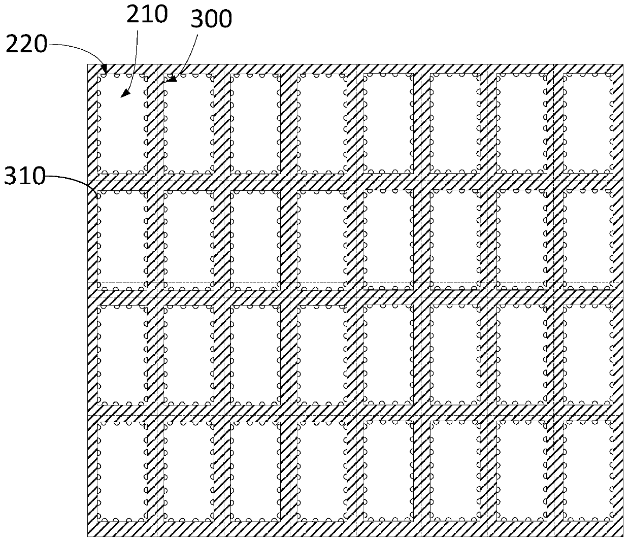
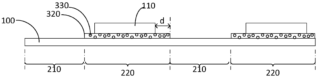
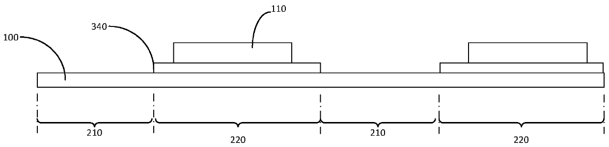
[0044] In order to make the purpose, technical solutions and advantages of the embodiments of the present disclosure clearer, the technical solutions of the embodiments of the present disclosure will be clearly and completely described below in conjunction with the accompanying drawings of the embodiments of the present disclosure. Apparently, the described embodiments are some of the embodiments of the present disclosure, not all of them. Based on the described embodiments of the present disclosure, all other embodiments obtained by persons of ordinary skill in the art without creative effort fall within the protection scope of the present disclosure.

[0045] Unless otherwise defined, the technical terms or scientific terms used in the present disclosure shall have the usual meanings understood by those skilled in the art to which the present disclosure belongs. "First", "second" and similar words used in the present disclosure do not indicate any order, quantity or importan...


PUM

PropertyMeasurementUnit
thicknessaaaaaaaaaa
thicknessaaaaaaaaaa

Abstract

The embodiment of the invention provides a transparent display device, a simulation method and a manufacturing method; the transparent display device comprises a substrate and a plurality of pixels distributed on the substrate in an array; and each pixel comprises a transparent area and a display area; and a scattering structure used for scattering light is arranged along the boundary line betweenthe transparent area and the display area. According to the transparent display device, the simulation method and the manufacturing method provided by the embodiment of the invention, the diffractionghosting phenomenon can be improved.

Description

technical field [0001] The invention relates to the field of display technology, in particular to a transparent display device, a simulation method and a manufacturing method. Background technique [0002] In related technologies, high PPI (Pixels Per Inch, pixel density) transparent display products are all small-sized LTPS-LED (low temperature polysilicon liquid crystal display), Mico-LED (micro liquid crystal display) or small-sized oxide OLED (oxide organic light emitting diode). Most of the large-size transparent display products are low PPI. For high-PPI large-size transparent display products, although there is a large market demand, there are still technical difficulties in related technologies that need to be overcome. [0003] A bottleneck of large-size high-PPI oxide OLED transparent display is that with the increase of PPI, the smaller the pixel size, the higher the metal wiring density, the smaller the transparent area, which affects the transmittance and is m...

Claims


Application Information

Patent Timeline
Patent Type & Authority Applications(China)
IPC IPC(8): H01L51/52H01L27/32H01L21/77G06F30/20
CPCG06F30/20H10K59/12H10K50/854H10K59/1201H10K71/00
Inventor 孙雪菲柳在健张星林奕呈徐攀韩影王国英高展
Owner BOE TECH GRP CO LTD
Why Eureka
Try Eureka