Ray emission area image measuring device and method

A technology of ray emission and image measurement, which is applied in the field of image measurement in the ray emission area, can solve the problems that the single-hole structure cannot meet the requirements of image measurement, the single-hole structure has insufficient field of view, and reduces the accuracy of measurement, etc. Limitation of field range, improvement of tolerance, and effect of simplified design

Active Publication Date: 2020-09-01
LASER FUSION RES CENT CHINA ACAD OF ENG PHYSICS
View PDF5 Cites 2 Cited by
  • Summary
  • Abstract
  • Description
  • Claims
  • Application Information

AI Technical Summary

Problems solved by technology

When any one of the above-mentioned single holes is used as the imaging component, it is the imaging component of the single-hole imaging diagnosis technology. Meet the requirements of laser-driven fusion neutron emission region image measurement
In order to solve the problem of insufficient field of view of the single-hole structure, the imaging component has evolved from a single-hole structure to a multi-type porous array structure, including multiple penumbral holes or multiple pinholes, etc. Although the porous array structure can meet the needs of laser-driven fusion The requirements for image measurement of the sub-emission area, however, its application range is greatly limited, and it is only applicable to neutron yields exceeding 1×10 14 The MJ-class laser device, resulting in the application of pinhole imaging diagnostic technology is limited by the neutron yield, reducing the accuracy of the measurement

Method used


Image

  • Ray emission area image measuring device and method
  • Ray emission area image measuring device and method
  • Ray emission area image measuring device and method

Examples


Embodiment 1

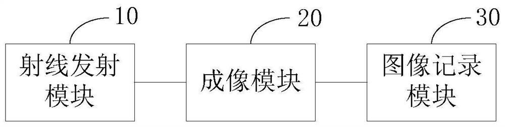
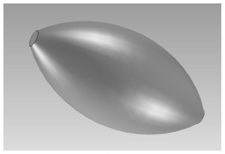
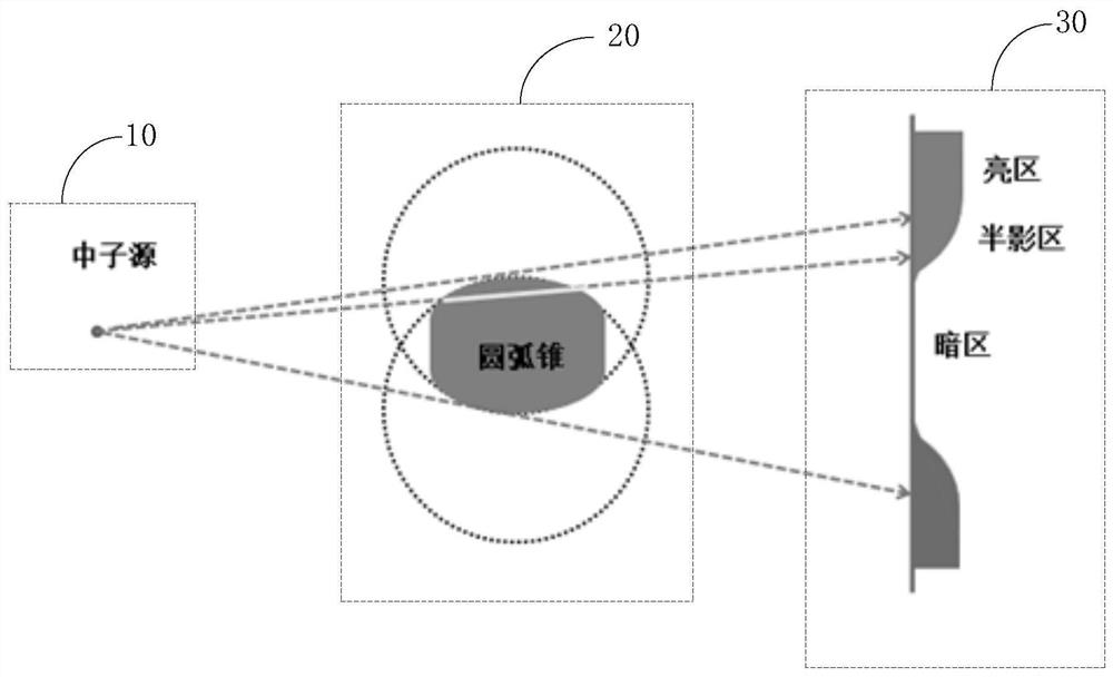
[0042] An embodiment of the present invention provides an image measuring device for a ray emitting area, figure 1 A schematic diagram of an image measurement device for a ray emitting area provided by an embodiment of the present invention, such as figure 1 As shown, the device includes: a ray emitting module 10, an imaging module 20 and an image recording module 30 arranged in sequence; wherein, the imaging module 20 is provided with an arc cone.

[0043] Wherein, the ray emitting module 10 is used to generate the ray, and send the ray to the image recording module 30 through the arc cone according to a preset trajectory, so that the image recording module 30 generates a measurement image according to the ray. Here, the imaging module 20 adopts an arc cone, which simplifies the design, processing and detection of the imaging module and reduces the aiming accuracy compared with the existing single hole structure and multi-type porous array structure. In addition, the ray poi...


PUM


Abstract

The invention provides a ray emission area image measuring device and method. The ray emission area image measuring device comprises a ray emitting module, an imaging module, and an image recording module, which are sequentially arranged; the imaging module is provided with an arc cone; the ray emitting module is used for generating rays and sending the rays to the image recording module through the arc cone according to a preset track, so that the image recording module generates a measurement image according to the rays. According to the invention, the arc cone is used as an imaging module;the design, processing and detection of the imaging module are simplified; the aiming precision is reduced; the limitation of the view field range of the existing ray emission area image detection technology is broken through; the requirement on the ray yield is reduced; the tolerance to random movement of the emission area ray source position is improved; meanwhile, the high spatial resolution capability is ensured; and the measurement precision is improved.

Description

technical field [0001] The invention relates to the technical field of measurement of images of radiation emission areas, in particular to an image measurement device and method of radiation emission areas. Background technique [0002] Radiation devices are widely used in many fields of scientific research and industrial production. Commonly used radiation devices include accelerator neutron sources, hash neutron sources, neutron tubes, reactors, synchrotron radiation devices, and radioisotope sources. The types of radiation include neutron , gamma rays, and X-rays. At present, as a new type of radiation device, a large-scale laser device has the characteristics of small size, short duration and high radiation flux. It can simultaneously generate neutrons, protons, gamma rays and X-rays, and has strong application potential. . In practical applications, in order to effectively use various radiation devices, it is necessary to understand the properties of the radiation sou...

Claims


Application Information

Patent Timeline
Patent Type & Authority Applications(China)
IPC IPC(8): G01T1/29
CPCG01T1/2992
Inventor 陈忠靖王峰郑建华江少恩张兴蒲昱东晏骥董云松余波
Owner LASER FUSION RES CENT CHINA ACAD OF ENG PHYSICS
Why Eureka
Try Eureka