Diffraction grating design method and system

A diffraction grating and design method technology, applied in the field of semiconductors, can solve the problems of destroying even diffraction orders and missing orders, reducing the contrast of measurement signals, etc., so as to avoid a large number of calculations.

Active Publication Date: 2020-09-01
INST OF MICROELECTRONICS CHINESE ACAD OF SCI
View PDF7 Cites 3 Cited by
  • Summary
  • Abstract
  • Description
  • Claims
  • Application Information

AI Technical Summary

Problems solved by technology

At present, when designing phase grating marks with high diffraction order enhancement, subdivision is usually used to enhance the required diffraction order. However, this method destroys the condition of even diffraction order deficiency while enhancing the required diffraction order. Causes even diffraction order diffraction signals, especially strong zero-order signals, reducing the contrast of the measured signal

Method used


Image

  • Diffraction grating design method and system
  • Diffraction grating design method and system
  • Diffraction grating design method and system

Examples


Embodiment Construction

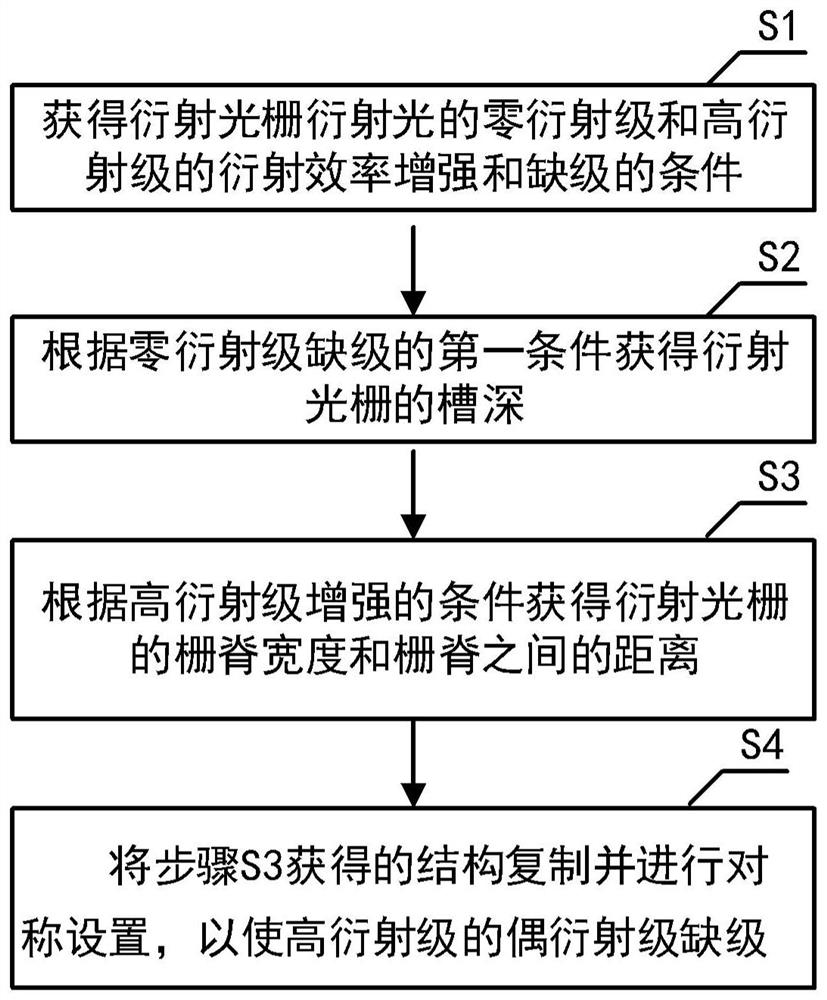
[0031] This publication provides a method and system for designing a diffraction grating, which solves the problem of a large amount of calculation in the process of scanning the grating marking. The method is firstly based on the conditions of each diffraction order enhancement and lack of order, and then according to the phase grating required enhancement and For the diffraction order of lack of order, select the grid level width and position information that meet the requirements, and obtain the phase grating structure that meets the requirements. This method selects the corresponding grid level and grid groove width and position according to the diffraction order that needs to be enhanced. It is necessary to set the entire grating structure as the optimization condition for optimization, avoiding a large number of calculations.

[0032] The present disclosure provides a method for designing a diffraction grating, such as figure 1 As shown, it includes: S1, the conditions f...


PUM


Abstract

The invention provides a design method and system of a diffraction grating. The method comprises the steps of S1 obtaining conditions of diffraction efficiency enhancement and default of a zero diffraction order and a high diffraction order of diffraction light of the diffraction grating; S2 obtaining the groove depth of the diffraction grating according to a first condition of zero diffraction order default; S3 obtaining the grid ridge width of the diffraction grating and the distance between grid ridges according to the condition of high diffraction order enhancement; and S4 copying the structure obtained in the step S3, and carrying out symmetrical arrangement, so that the even diffraction order of the high diffraction order is lack of order. According to the method, the widths and thepositions of the corresponding grid level and the grid groove are selected according to the diffraction order needing to be enhanced, the whole grating structure does not need to be set as an optimization condition to be optimized, and a large amount of calculation is avoided.

Description

technical field [0001] The present application relates to the field of semiconductor technology, in particular to a method and system for designing a diffraction grating. Background technique [0002] In the field of semiconductor, integrated circuit and mirror displacement measurement, position measurement sensors based on phase gratings are often used to determine the position information of the target. During the measurement, the low diffraction order is used to capture the grating, and the high diffraction order is used to improve the measurement accuracy. Due to the limitation of grating diffraction characteristics, the diffraction efficiency of high diffraction order is low, and due to the influence of grating processing error and process, the diffraction efficiency of high diffraction order is further reduced. When the diffraction efficiency is lower than a certain threshold, it will lead to measurement repeatability The sharp decrease, even the high diffraction orde...

Claims


Application Information

Patent Timeline
Patent Type & Authority Applications(China)
IPC IPC(8): G02B5/18
CPCG02B5/18
Inventor 李璟杨光华卢增雄张清洋丁敏侠
Owner INST OF MICROELECTRONICS CHINESE ACAD OF SCI
Why Eureka
Try Eureka