Mini light emitting diode backlight module, manufacturing method thereof and display device

A technology of light-emitting diodes and backlight modules, which is applied in electrical components, electric solid-state devices, circuits, etc., can solve problems such as energy waste, and achieve the effect of solving energy waste and good thermal conductivity.

Inactive Publication Date: 2020-09-01
SHENZHEN CHINA STAR OPTOELECTRONICS SEMICON DISPLAY TECH CO LTD
View PDF7 Cites 1 Cited by
  • Summary
  • Abstract
  • Description
  • Claims
  • Application Information

AI Technical Summary

Problems solved by technology

[0005] This application provides a mini light-emitting diode backlight module, its manufacturing method and display device, which can solve the technical problem of energy waste caused by high-temperature reflow soldering in the existing die-bonding process

Method used


Image

  • Mini light emitting diode backlight module, manufacturing method thereof and display device
  • Mini light emitting diode backlight module, manufacturing method thereof and display device
  • Mini light emitting diode backlight module, manufacturing method thereof and display device

Examples


Embodiment Construction

[0040] The following will clearly and completely describe the technical solution in the application with reference to the accompanying drawings in the implementation manner of the application. Apparently, the described implementations are only some of the implementations of this application, not all of them. Based on the implementation manners in this application, all other implementation manners obtained by those skilled in the art without creative efforts shall fall within the scope of protection of this application.

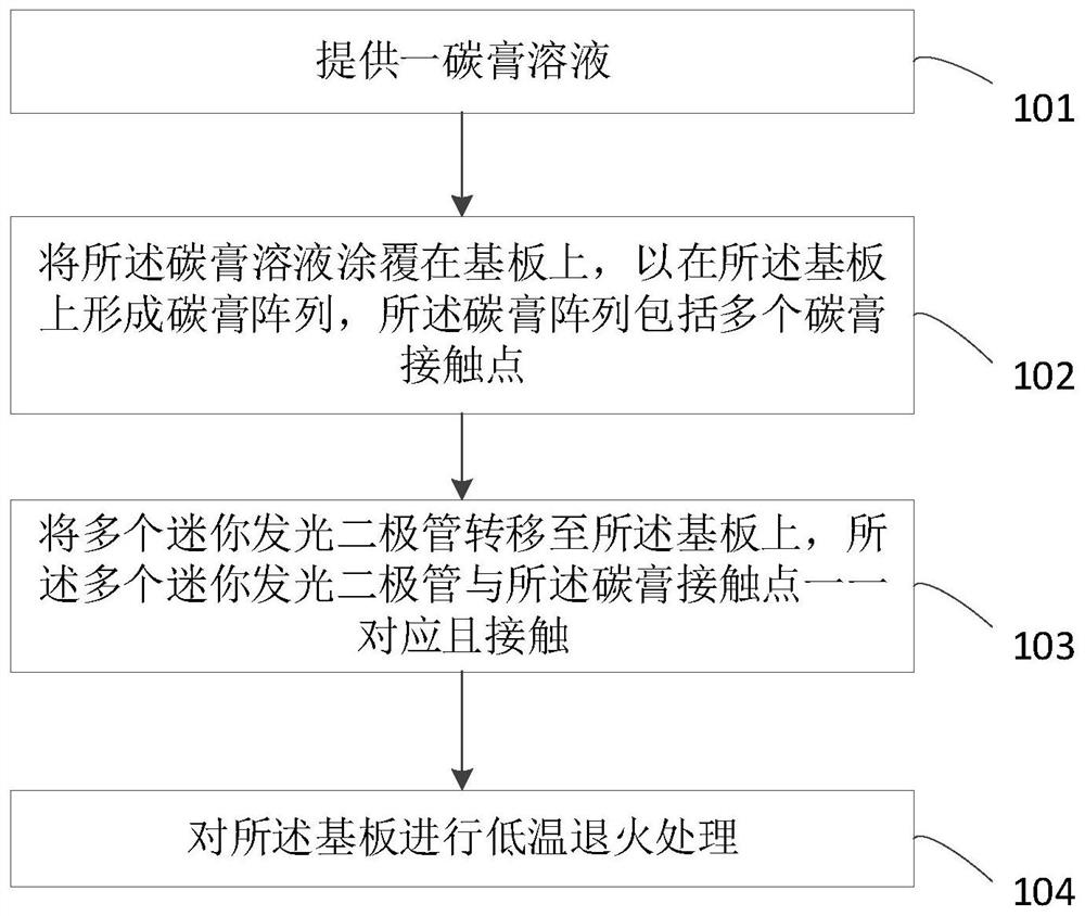
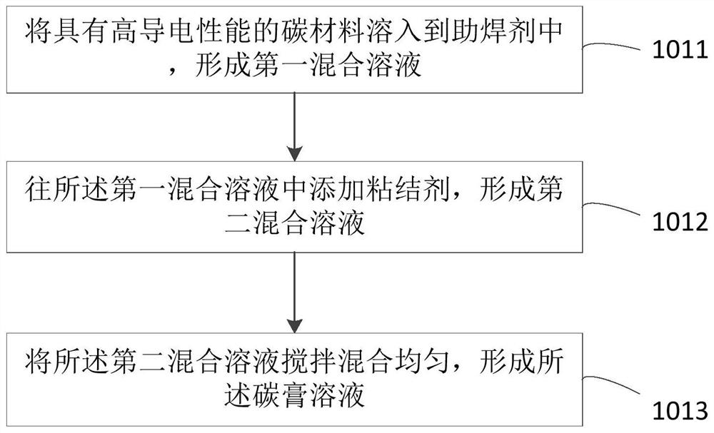
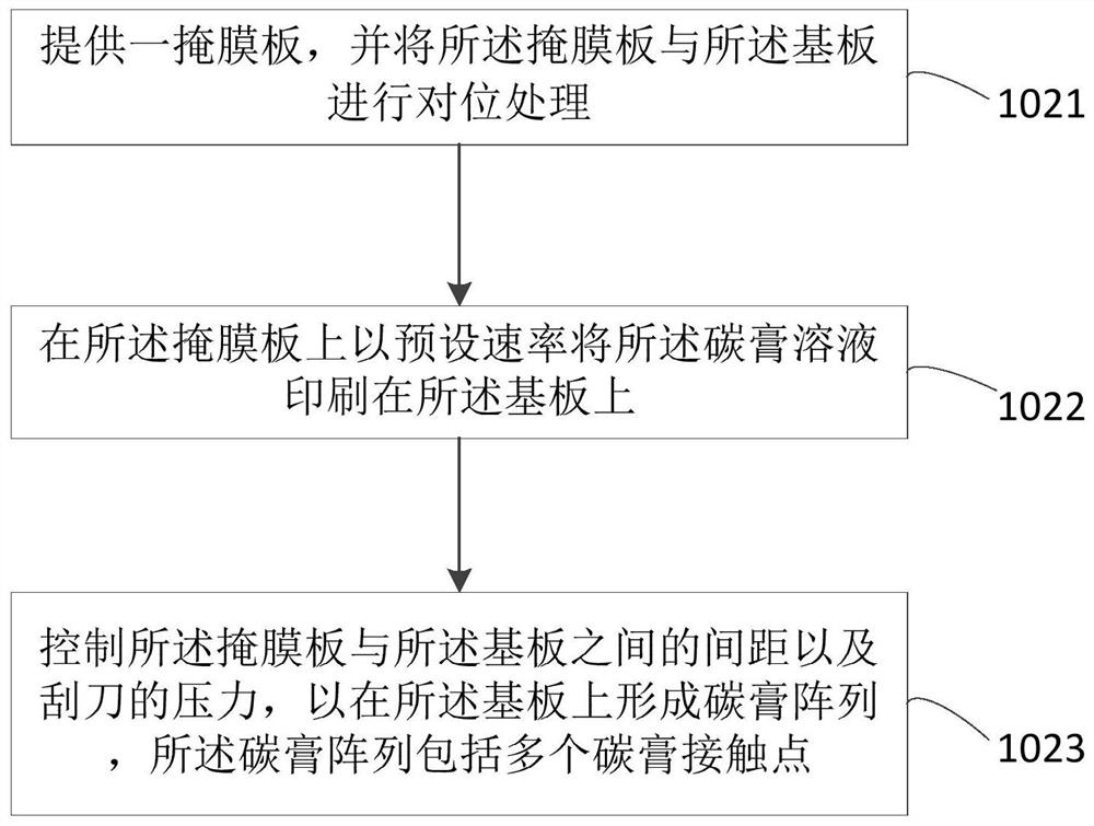
[0041] see figure 1 , figure 1 It is a schematic flowchart of the manufacturing method of the mini LED backlight module provided by the embodiment of the present application. Such as figure 1 As shown, the manufacturing method of the mini light-emitting diode backlight module provided by the embodiment of the present application includes the following steps: 101, providing a carbon paste solution; 102, coating the carbon paste solution on a substrate, so th...


PUM


Abstract

The invention provides a mini light-emitting diode backlight module, a manufacturing method thereof and a display device. The manufacturing method comprises the steps of providing a carbon paste solution; coating a substrate with the carbon paste solution to form a carbon paste array on the substrate, wherein the carbon paste array comprises a plurality of carbon paste contact points; transferringa plurality of mini light-emitting diodes to the substrate, wherein the plurality of mini light-emitting diodes are in one-to-one correspondence and contact with the plurality of carbon paste contactpoints; and carrying out a die bonding method, namely, low-temperature annealing treatment on the substrate. The high-conductivity carbon paste is used for replacing solder paste to serve as a die bonding raw material, high-temperature reflow soldering is not adopted, and the die bonding process is completed through low-temperature sintering, so that the die bonding process is simpler and more energy-saving, and the technical problem of energy waste caused by high-temperature reflow soldering adopted in an existing die bonding process can be solved.

Description

technical field [0001] The present application relates to the field of display, in particular to a mini LED backlight module, a manufacturing method thereof and a display device. Background technique [0002] At present, as a cold light source, a light emitting diode (Light Emitting Diode, LED) has the advantages of environmental protection and energy saving, and has been widely used in lighting. At the same time, LEDs are gradually being used in the field of display panels, such as LED screen billboards, due to their high brightness, long life, and wide viewing angles. In particular, the application of mini light-emitting diodes (mini LEDs) in the field of display lighting has become a recent research hotspot and has attracted the attention of major panel manufacturers. In the production process of mini light-emitting diode display modules, die bonding is very important. Core process. [0003] Wherein, for mini LEDs, solder paste is generally used as the solder for die bo...

Claims


Application Information

Patent Timeline
IPC IPC(8): H01L33/48H01L33/62H01L27/15
CPCH01L27/156H01L33/48H01L33/62H01L2933/0033H01L2933/0066
Inventor 段淼
Owner SHENZHEN CHINA STAR OPTOELECTRONICS SEMICON DISPLAY TECH CO LTD
Why Eureka
Try Eureka