
Transistor, three dimensional memory device including such transistor and method of fabricating such memory device

A technology for memory cells and transistors, which is applied in semiconductor/solid-state device manufacturing, transistors, electric solid-state devices, etc., can solve the problem that three-dimensional memory elements cannot use vertical current type sector field effect transistors, etc., and achieve the effect of improving cell density.

Inactive Publication Date: 2020-09-04
王振志
View PDF1 Cites 0 Cited by
  • Summary
  • Abstract
  • Description
  • Claims
  • Application Information

AI Technical Summary

Problems solved by technology

[0006] However, vertical current mode Sector Field Effect Transistors cannot be used for three-dimensional memory elements that require current flow in the horizontal direction

Method used


Image

  • Transistor, three dimensional memory device including such transistor and method of fabricating such memory device
  • Transistor, three dimensional memory device including such transistor and method of fabricating such memory device
  • Transistor, three dimensional memory device including such transistor and method of fabricating such memory device

Examples


Embodiment Construction

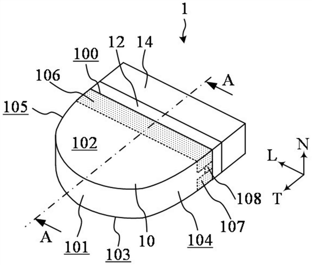
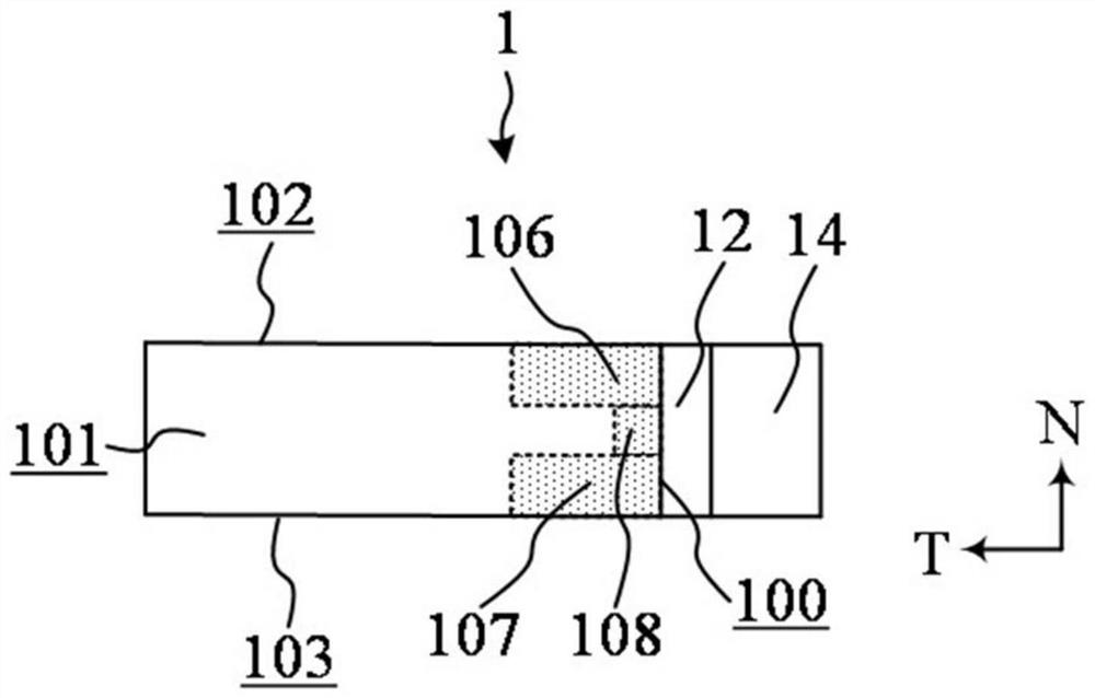
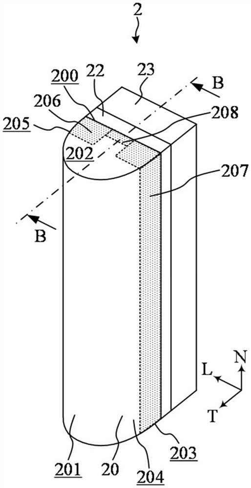
[0089] see image 3 and Figure 4 , these figures schematically depict a transistor 2 according to a preferred embodiment of the present invention. image 3 A transistor 2 according to a preferred embodiment of the present invention is schematically shown in an external view. Figure 4 image 3 A cross-sectional view of middle transistor 2 along line B-B.

[0090] Such as image 3 and Figure 4 As shown, the transistor 2 (also referred to as “horizontal current mode field effect transistor”) according to the preferred embodiment of the present invention includes a pillar 20 formed of semiconductor material, a gate dielectric layer 22 and a gate conductor 23 .

[0091] A pillar 20 formed of semiconductor material is formed along a semiconductor substrate (not shown in image 3 and Figure 4 ) extends in the normal direction N. A column 20 formed of semiconductor material has a base side 200 parallel to the normal direction N of the semiconductor substrate, a tapered sid...


PUM


Abstract

The invention discloses a transistor, a three dimensional memory device including such transistors and a method of fabricating such memory device. The transistor according to the invention includes apillar of a semiconductor material, extending in a normal direction of a semiconductor substrate, a gate dielectric layer and a gate conductor. The pillar of the semiconductor material has a base sideface parallel to the normal direction, a tapered side face opposite to the base side face, a top face perpendicular to the normal direction, a bottom face opposite to the top face, a front side faceadjacent to the base side face and the tapered side face, and a rear side face opposite to the front side face. A first elongated portion, sandwiched among the base side face, the front side face, thebottom face and the top face, forms a source region. A second elongated portion, sandwiched among the base side face, the rear side face, the bottom face and the top face, forms a drain region. A plate portion, on the base side face and between the first elongated portion and the second elongated portion, forms a channel region. Other portion of the pillar forms a body region. The gate dielectriclayer is formed to overlay the base side face of the pillar of the semiconductor material. The gate conductor is formed to overlay the gate dielectric layer.

Description

technical field [0001] The invention relates to a transistor, a three-dimensional memory element including the transistor and a method for manufacturing the memory element, in particular to a novel transistor, a three-dimensional memory element including the transistor and a method for manufacturing the memory element. Background technique [0002] see figure 1 and figure 2 , these figures schematically depict a vertical current mode fan-shaped field effect transistor (fan-shaped field effect transistor, FanFET) 1 disclosed by US Patent Application Publication No. 2019123060A1. figure 1 It is an external view of the vertical current mode sector field effect transistor 1 . figure 2 yes figure 1 A cross-sectional view of a medium vertical current mode Sector Field Effect Transistor 1 along line A-A. [0003] Such as figure 1 and figure 2 As shown, the conventional vertical current mode sector field effect transistor 1 includes a pillar 10 formed of semiconductor mater...

Claims


Application Information

Patent Timeline
Patent Type & Authority Applications(China)
IPC IPC(8): H01L29/06H01L29/08H01L29/78H01L27/11524H01L27/11551H01L27/1157H01L27/11578H10B43/27H10B41/10H10B41/20H10B41/27H10B41/35H10B43/20H10B43/35
CPCH01L29/0657H01L29/78H01L29/0847H10B41/20H10B41/35H10B43/20H10B43/35H10B43/10H10B43/27H01L29/792H01L29/788H10B41/10H10B41/27H01L29/1037H01L29/513H01L23/528H01L21/31111H01L21/76224H01L21/02532H01L29/40114H01L21/32133H01L29/40117H01L21/30604
Inventor 王振志何立玮王宇扬
Owner 王振志
Features
  • Generate Ideas
  • Intellectual Property
  • Life Sciences
  • Materials
  • Tech Scout
  • Unparalleled Data Quality
  • Higher Quality Content
  • 60% Fewer Hallucinations
Learn More