Semiconductor device testing device

A testing device and semiconductor technology, applied in the direction of single semiconductor device testing, measuring devices, components of electrical measuring instruments, etc., can solve the problem of low testing efficiency of semiconductor devices, reduce company operating costs, save labor costs, and improve testing The effect of efficiency

Pending Publication Date: 2020-09-08
YANGZHOU HY TECH DEV
View PDF0 Cites 5 Cited by
  • Summary
  • Abstract
  • Description
  • Claims
  • Application Information

AI Technical Summary

Problems solved by technology

[0005] The present application solves the problem of low testing efficiency of semiconductor devices in the prior art by providing a semiconductor device testing device, and greatly improves the testing efficiency of semiconductor devices

Method used


Image

  • Semiconductor device testing device
  • Semiconductor device testing device
  • Semiconductor device testing device

Examples


Embodiment 1

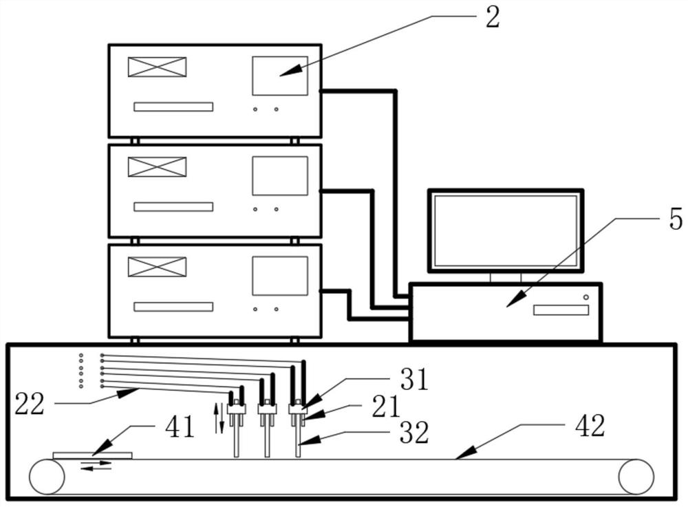
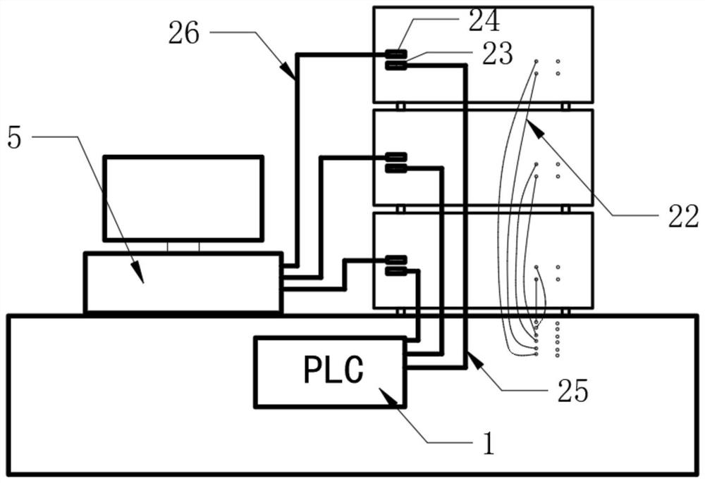
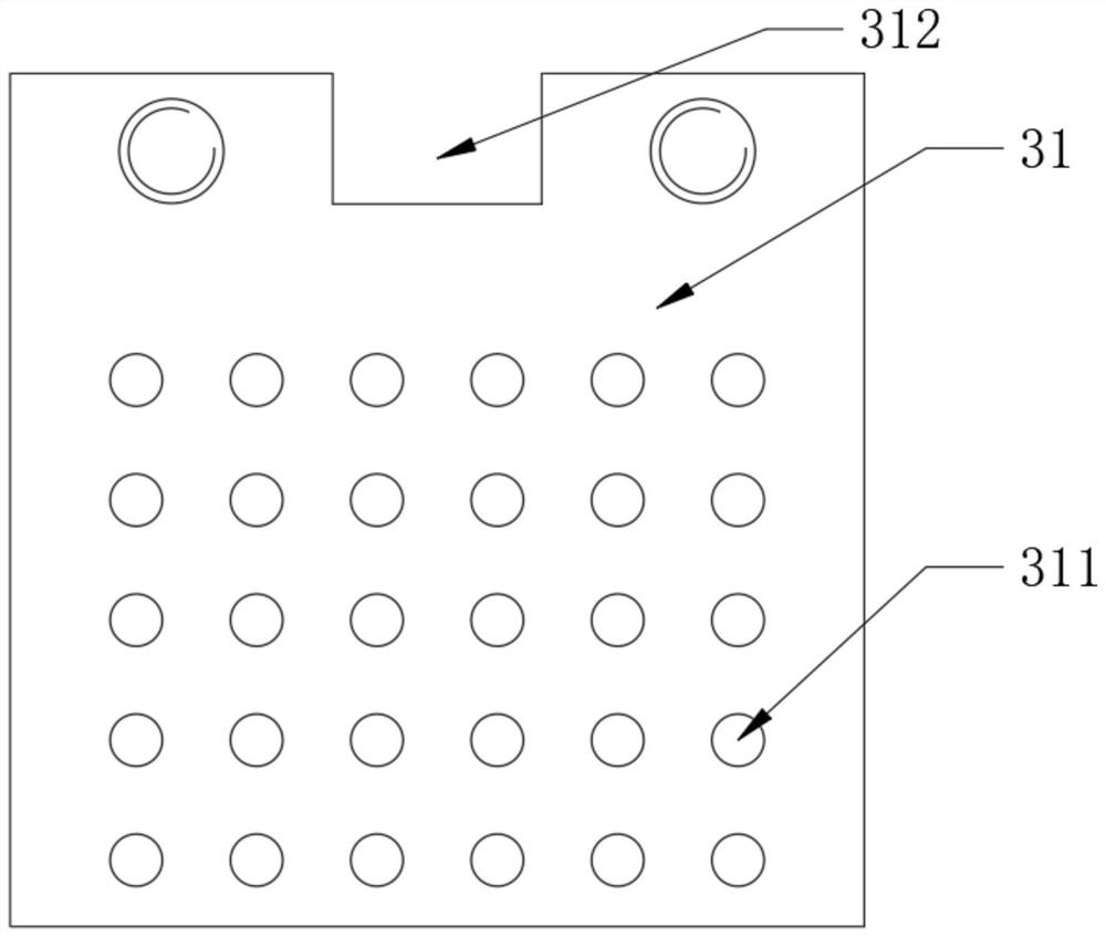
[0046] Such as Figure 1-5As shown, the embodiment of the present application provides a semiconductor device testing device, comprising: a PLC controller 1, a testing machine 2, a probe fixing unit, a carrying unit and a computer; The back side of machine 2 is provided with PIN15 interface 23 and PIN25 interface 24, and the PIN15 interface 23 of testing machine 2 is connected with PLC controller 1 by PIN15 data transmission line 25, and the PIN25 interface 24 of testing machine 2 is connected with computer 5 by PIN25 data transmission line 26, and computer 5 is used to collect and process the test data of the testing machine 2; the probe fixing unit includes a probe base 31 and a lifting mechanism, the lifting mechanism is a hydraulic cylinder (not shown in the figure), and the telescopic end of the hydraulic cylinder is affixed to the probe base 31 , the probe holder 31 is provided with a plurality of through holes 311 arranged in a square array, the distance between adjacen...


PUM


Abstract

The invention discloses a semiconductor device testing device in the technical field of semiconductor devices. The testing device comprises a testing machine which is used for testing the performanceof a semiconductor device; a probe fixing unit which is used for fixing a probe of the testing machine and driving the probe to move in the vertical direction; a bearing unit which is located under the probe fixing unit, and used for bearing the semiconductor device and driving the semiconductor device to move in the horizontal direction; and a PLC which is electrically connected with the testingmachine, the probe fixing unit and the bearing unit and controls the testing machine, the probe fixing unit and the bearing unit to work. According to the semiconductor device testing device, the testing machine is controlled by the PLC to test the semiconductor devices passing through the lower parts of the probes one by one; automatic testing of multiple packaged semiconductor devices on a largescale is achieved, the assembling and disassembling time during testing of the semiconductor devices is saved, the testing efficiency of the semiconductor devices on a large scale is improved, the labor cost is reduced, and the company operation cost is reduced.

Description

technical field [0001] The invention relates to the technical field of semiconductor devices, in particular to a semiconductor device testing device. Background technique [0002] With the development of society and the advancement of technology, semiconductor devices need to be electrically tested after production to ensure that they can meet the requirements. [0003] The current small-batch electrical performance verification of semiconductor devices is conducted by manually operating the testing machine to test the electrical performance of semiconductor devices. A single testing machine has a single test item and needs to cooperate with multiple types of testing machines to complete a series of electrical performance tests. Since the testing machine can only test A semiconductor device, so when faced with a large number of semiconductor devices to be tested, it is necessary to manually load and unload semiconductor devices repeatedly. The test efficiency is low, which l...

Claims


Application Information

Patent Timeline
Patent Type & Authority Applications(China)
IPC IPC(8): G01R31/26G01R31/01G01R1/073
CPCG01R1/073G01R31/01G01R31/2601
Inventor 林俊
Owner YANGZHOU HY TECH DEV
Why Eureka
Try Eureka