Upper electrode uncovering structure and semiconductor processing equipment

A technology for processing equipment and electrodes, which is applied in semiconductor/solid-state device manufacturing, circuits, electrical components, etc., and can solve problems such as radio frequency leakage, affecting process results, and poor conduction between the upper electrode and the chamber

Active Publication Date: 2020-09-08
BEIJING NAURA MICROELECTRONICS EQUIP CO LTD
View PDF7 Cites 0 Cited by
  • Summary
  • Abstract
  • Description
  • Claims
  • Application Information

AI Technical Summary

Problems solved by technology

After the cleaning of the chamber is completed, the upper electrode needs to be dropped on the chamber through the cover opening mechanism, but due to the phenomenon of "overhead", the upper electrode on the side far away from the cover mechanism will first contact the upper surface of the chamber, resulting in the bottom of the upper electrode The inductive coil in contact with the chamber produces a lateral force, which causes the inductive coil to deform. Multiple cumulative deformations will seriously affect the conductive function of the inductive coil, resulting in the failure of good conduction between the upper electrode and the chamber. At the same time, the upper electrode and the chamber RF leakage can occur at the gap of the chamber contact surface, which can affect the process result

Method used


Image

  • Upper electrode uncovering structure and semiconductor processing equipment
  • Upper electrode uncovering structure and semiconductor processing equipment
  • Upper electrode uncovering structure and semiconductor processing equipment

Examples


Embodiment Construction

[0038] Specific embodiments of the present invention will be described in detail below in conjunction with the accompanying drawings. It should be understood that the specific embodiments described here are only used to illustrate and explain the present invention, and are not intended to limit the present invention.

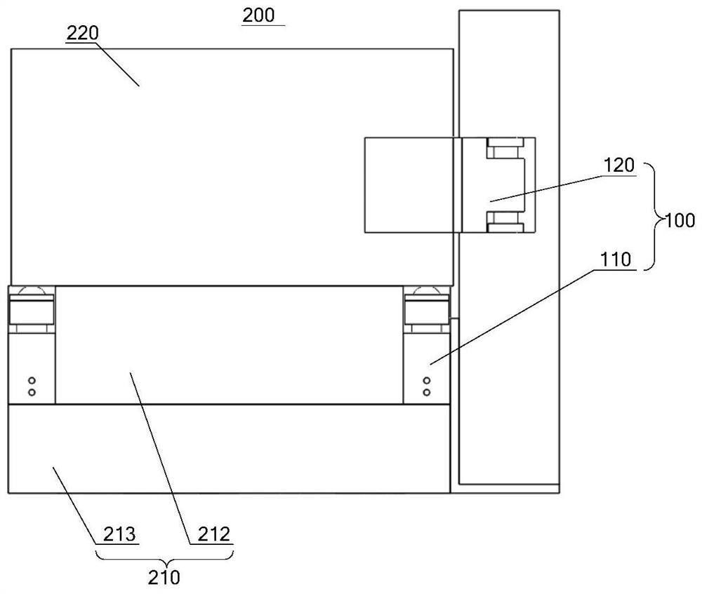
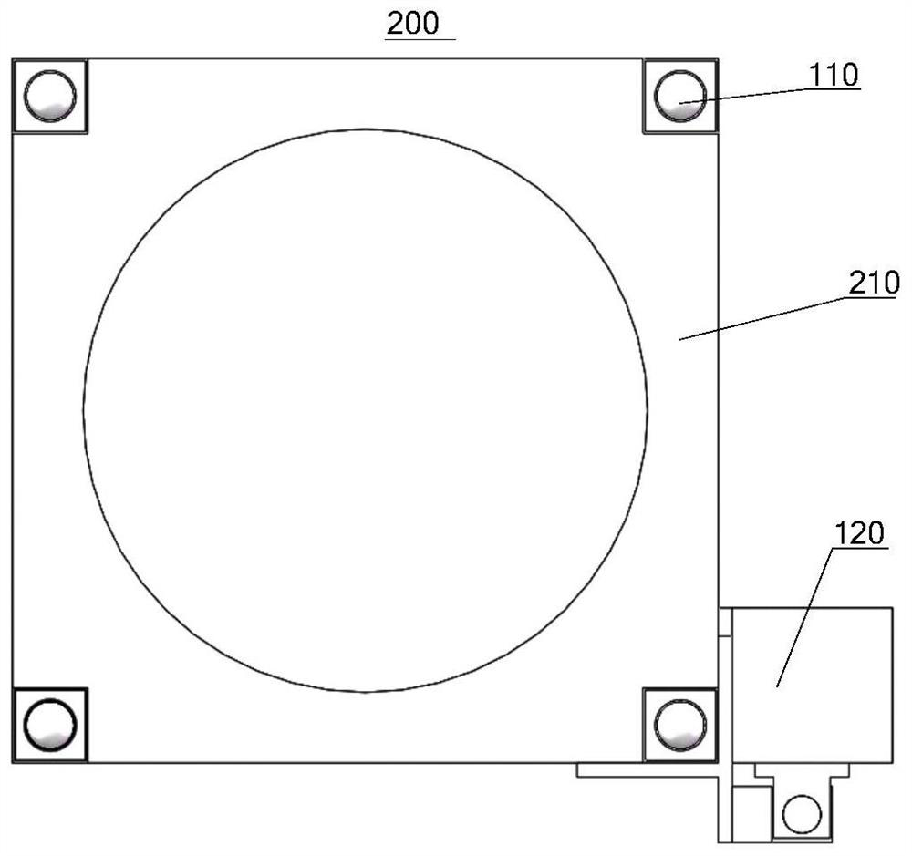
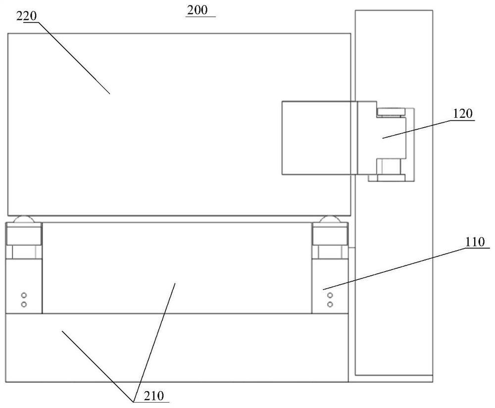
[0039] see figure 1 and figure 2 , a semiconductor processing equipment 200, the semiconductor processing equipment 200 includes a chamber 210, an upper electrode 220 located at the top of the chamber 210, a lower electrode (not shown in the figure) located at the bottom of the chamber 210, and an opening structure 100. An inductive coil (not shown) is provided between the upper electrode 220 and the top of the chamber 210; the inductive coil is connected to the bottom of the upper electrode 220, and rises and falls together with the upper electrode 220 when the cover is opened, or is connected to the chamber. 210 top. The cover opening structure 100 include...


PUM


Abstract

The invention discloses an upper electrode uncovering structure and semiconductor processing equipment. The uncovering structure comprises a first lifting mechanism located below the upper electrode,wherein the first lifting mechanism can independently drive the upper electrode to ascend and descend in the vertical direction in a preset first lifting stage and keep the whole upper electrode in ahorizontal state, so that the upper electrode is switched between a process position and an initial cover opening position; a second lifting mechanism which is located on the side of the upper electrode and connected with the upper electrode, wherein the second lifting mechanism can independently drive the upper electrode to ascend and descend in the vertical direction in a preset second lifting stage, so that the upper electrode is switched between the initial uncovering position and the target uncovering position, and the initial uncovering position is located between the process position and the target uncovering position. The conductive function of the induced coil can be remarkably improved, good electrical conduction between the upper electrode and the cavity is effectively guaranteed, meanwhile, radio frequency leakage can be avoided, and the process result is improved.

Description

technical field [0001] The invention relates to the technical field of semiconductor equipment, in particular to an upper electrode cover opening structure and a semiconductor processing equipment. Background technique [0002] The process module of PSS etching machine is composed of upper and lower electrodes. The upper electrode is mainly composed of upper matching device, coil system and quartz cover. The lower electrode is mainly composed of lower matching device, chuck and other components. During the process, the upper electrode is loaded A certain power ionizes the incoming process gas, and then bombards the wafer placed on the lower electrode chuck. After the ion bombards the wafer, a large number of by-products will be produced, and most of the by-products will be dry-pumped to the exhaust gas of the factory through the molecular pump. Processing equipment, but some of the by-products will adhere to the chamber and the quartz cover, and the accumulation of by-produc...

Claims


Application Information

Patent Timeline
Patent Type & Authority Applications(China)
IPC IPC(8): H01L21/67
CPCH01L21/67H01L21/67011Y02P70/50
Inventor 罗大龙
Owner BEIJING NAURA MICROELECTRONICS EQUIP CO LTD
Why Eureka
Try Eureka