On-chip transformer-based transmission zero tunable filter

An on-chip transformer, transmission zero technology, applied in the field of filters, can solve the problems of poor passband selectivity, small size, no transmission zero and tunability, etc., to achieve compact circuit model, high space utilization, and tunable. sexual effect

Active Publication Date: 2021-06-11
NANJING UNIV OF SCI & TECH
View PDF6 Cites 0 Cited by
  • Summary
  • Abstract
  • Description
  • Claims
  • Application Information

AI Technical Summary

Problems solved by technology

[0003] Chinese patent 201822061717.3 discloses an improved on-chip second-order bandpass filter, in the frequency range of 30GHz to 55GHz,|S 11 The values ​​of | are all below -10dB, and there are two obvious resonance points, and the volume is small, easy to integrate with other devices, but its passband selectivity is poor, there is only one transmission zero point on the right side of the passband and away from the passband take far
[0004] Yang Yang and other researchers published a paper entitled "Compact On-Chip Bandpass Filter With Improved In-Band Flatness and Stopband Attenuation in 0.13-μm(Bi)-CMOS Technology" on IEEE ELECTRON DEVICE LETTERS. A center-tapped ring resonator and a parallel capacitor-loaded bandpass filter, in the frequency range of 28GHz to 42GHz, |S 11 The values ​​of | are all below -10dB, and there are two obvious resonance points. Its design idea is novel, and it cleverly uses the on-chip MIM capacitor loading, but its passband selectivity is poor, and it does not have transmission zero point and adjustability.

Method used


Image

  • On-chip transformer-based transmission zero tunable filter
  • On-chip transformer-based transmission zero tunable filter
  • On-chip transformer-based transmission zero tunable filter

Examples


Embodiment Construction

[0021] In order to make the purpose, technical solution and advantages of the present application clearer, the present application will be further described in detail below in conjunction with the accompanying drawings and embodiments. It should be understood that the specific embodiments described here are only used to explain the present application, and are not intended to limit the present application.

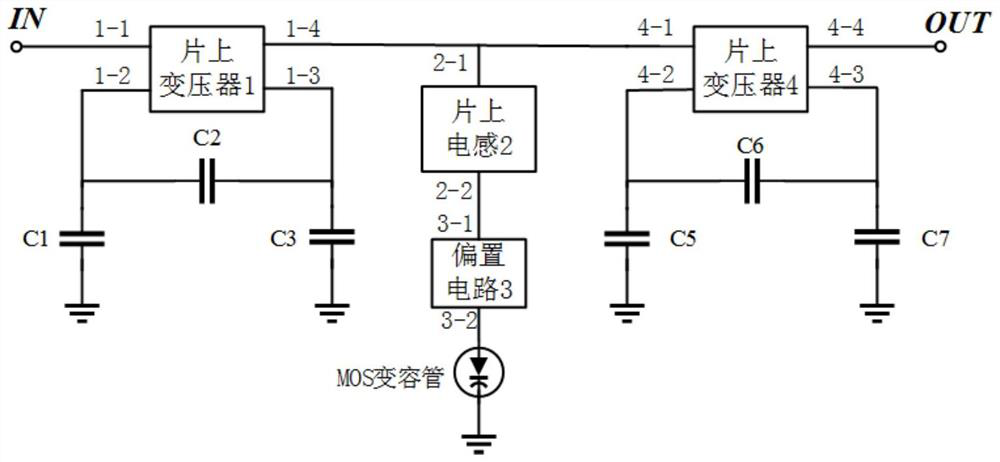
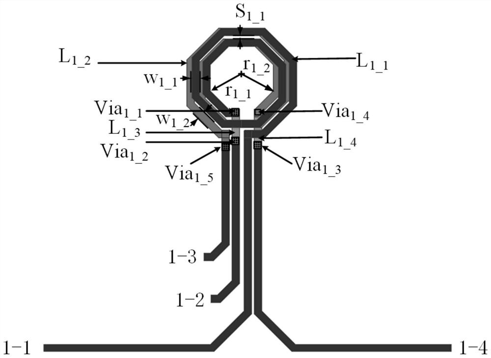
[0022] In one embodiment, combined with figure 1 , provides an on-chip transformer-based adjustable transmission zero filter, the filter includes a first on-chip transformer 1, an on-chip inductor 2, a bias circuit 3, a second on-chip transformer 4, a first capacitor C1, a second Capacitor C2, third capacitor C3, fifth capacitor C5, sixth capacitor C6, seventh capacitor C7 and MOS varactors;

[0023] The first port 1-1 of the first on-chip transformer 1 is used as the input port of the filter, the second port 1-2 is grounded through the first capacitor C1, the third port ...


PUM


Abstract

The invention discloses an on-chip transformer-based transmission zero-point adjustable filter, including first and second on-chip transformers, on-chip inductors, bias circuits, first to third capacitors, fifth to seventh capacitors, and MOS varactors; The first port of the on-chip transformer is used as the input end of the filter, the second and third ports are respectively grounded through the first and third capacitors, the second capacitor is connected across the second and third ports, and the fourth port is connected to the first capacitor of the on-chip inductor. One port and the first port of the second on-chip transformer; the second port of the on-chip inductor is connected to the first port of the bias circuit, the second port is connected to the positive pole of the MOS varactor, and the negative pole of the MOS varactor is grounded; the second on-chip transformer The second and third ports are respectively grounded through the fifth and seventh capacitors, the sixth capacitor is connected across the second and third ports, and the fourth port is used as the output end of the filter. The filter of the invention has the advantages of small size, flexible design, easy integration with other devices, etc., and can well meet the requirements of modern communication systems.

Description

technical field [0001] The invention relates to the field of filters, in particular to an on-chip transformer-based transmission zero-point adjustable filter. Background technique [0002] In the past decade, with the rapid development of emerging microwave technologies, the design of high-performance on-chip passive devices based on standard silicon (Si) technology has received great attention from scholars at home and abroad. Several new approaches to the realization of different on-chip passive devices, such as antennas, baluns, slow-wave transmission lines, and band-pass filters (BPFs), have recently been proposed in the literature. Microwave filter is an indispensable device in the transmitting and receiving ends of modern communication systems. It separates signals, allowing useful signals to pass through without attenuation as much as possible, and suppressing useless signals from passing through with as much attenuation as possible. The design of on-chip bandpass fi...

Claims


Application Information

Patent Timeline
Patent Type & Authority Patents(China)
IPC IPC(8): H01P1/203H01L23/64
CPCH01L23/64H01P1/203
Inventor 黄同德王奕吴文
Owner NANJING UNIV OF SCI & TECH
Why Eureka
Try Eureka