Method for manufacturing organic electroluminescent display device

An electroluminescence display, organic technology, applied in the direction of electric solid device, semiconductor/solid state device manufacturing, electrical components, etc., can solve the problems of low luminous efficiency, poor performance stability, low luminous brightness, etc., to achieve simple preparation process, luminous The effect of strength enhancement and overall performance improvement

Inactive Publication Date: 2010-06-16
IRICO
View PDF2 Cites 0 Cited by
  • Summary
  • Abstract
  • Description
  • Claims
  • Application Information

AI Technical Summary

Problems solved by technology

[0003] Aiming at the technical problems of low luminous brightness, low luminous efficiency and poor performance stability of organic electroluminescent display devices in the prior art, the present invention provides a method for preparing an organic electroluminescent display device, comprising the following steps:

Method used


Image

  • Method for manufacturing organic electroluminescent display device
  • Method for manufacturing organic electroluminescent display device

Examples


Embodiment 1

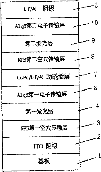
[0018] A method for preparing an organic electroluminescence display device includes the following steps:

[0019] 1) Print the indium tin oxide ITO anode 2 pattern of the organic electroluminescence display device OLED on the cleaned conductive substrate 1, and the substrate with the printed indium tin oxide ITO anode 2 pattern is ultrasonically cleaned with toluene, ethanol and acetone respectively. Dip and rinse with deionized water. Finally, an ozone ion bombardment treatment was performed in a vacuum chamber, the pressure was controlled at 50 Pa, and the substrate was bombarded for 20 minutes.

[0020] 2) Use vacuum evaporation method to evaporate hole transport layer material N,N'-bis(1-naphthyl)-N,N'-diphenyl- on the substrate with printed indium tin oxide ITO anode 2 pattern. 1,1'-Diphenyl-4,4'-diamine, referred to as NPB, prepares the first hole transport layer 3 of NPB, and the system vacuum is 5×10 -5 Pa, NPB deposition rate is 0.1nm / s, thickness is 80nm.

[0021] 3) On ...

Embodiment 2

[0030] A method for preparing an organic electroluminescence display device includes the following steps:

[0031] 1) Print the indium tin oxide ITO anode 2 pattern of the organic electroluminescence display device OLED on the cleaned conductive substrate 1, and the substrate with the printed indium tin oxide ITO anode 2 pattern is ultrasonically cleaned with toluene, ethanol and acetone respectively. Then immerse and rinse with deionized water, and then rinse with deionized water, then rinse with deionized water, then use toluene, ethanol and acetone for ultrasonic cleaning, and then rinse with deionized water, and finally in the vacuum chamber Carry out ozone ion bombardment treatment, control the pressure between 5 Pa, and bombard the substrate for 5 minutes.

[0032] 2) Use vacuum evaporation method to evaporate hole transport layer material N,N'-bis(1-naphthyl)-N,N'-diphenyl- on the substrate with printed indium tin oxide ITO anode 2 pattern. 1,1'-Diphenyl-4,4'-diamine, refer...

Embodiment 3

[0042] A method for preparing an organic electroluminescence display device includes the following steps:

[0043] 1) Print the indium tin oxide ITO anode 2 pattern of the organic electroluminescence display device OLED on the cleaned conductive substrate 1, and ultrasonically clean the substrate with the printed indium tin oxide ITO anode 2 pattern in deionized water with detergent , Then rinse with deionized water, then ultrasonically clean with toluene, ethanol, and acetone, then rinse with deionized water, and finally perform ozone ion bombardment treatment in a vacuum chamber, control the pressure at 30Pa, and perform the substrate Bombard for 15min.

[0044] 2) Use vacuum evaporation method to evaporate hole transport layer material N,N'-bis(1-naphthyl)-N,N'-diphenyl- on the substrate with printed indium tin oxide ITO anode 2 pattern. 1,1'-Diphenyl-4,4'-diamine, referred to as NPB, prepares the first hole transport layer 3 of NPB, and the system vacuum is 5×10 -5 Pa, NPB dep...


PUM

PropertyMeasurementUnit
luminanceaaaaaaaaaa

Abstract

The invention relates to a method for manufacturing an organic electroluminescent display device, belonging to the technical field of panel display and comprising the steps of: 1) printing an ITO anode graphics on a conductive substrate, ultrasonically cleaning the substrate printed with an anode for the ozone ion bombardment treatment in a vacuum chamber; 2) manufacturing an NPB cavity transportlayer on the substrate; 3) manufacturing a luminescent layer on the cavity transport layer; 4) manufacturing Alq3 electronic transport layer on the luminescent layer; 5) manufacturing a CuPc / LiF / Al functional intercalated layer on the electronic transport layer; 6) manufacturing a second cavity transport layer on the functional intercalated layer; 7) manufacturing a second luminescent layer on thesecond cavity transport layer; 8) manufacturing a second Alq3 electronic transport layer on the second luminescent layer; 9) manufacturing an LiF / Al mixed cathode on the second Alq3 electronic transport layer; and 10) integrally encapsulating the device with an encapsulating substrate to complete the manufacturing of the device. The inventive organic electroluminescent display device OLED has simple manufacturing technologies and can realize high-brightness narrow-band emission.

Description

Technical field [0001] The invention belongs to the technical field of flat panel displays, and relates to a method for preparing an organic electroluminescence display device. Background technique [0002] Organic electroluminescent display devices, or OLEDs for short, have become the most powerful device in the field of optoelectronic devices and flat panel displays because of their high luminous efficiency, low driving voltage, simple manufacturing process, low cost, ultra-thin, and surface emission and full-color display. One of the promising technologies. Generally, the organic electroluminescence display device is composed of a substrate, an indium tin oxide ITO anode, an NPB hole transport layer, and a vapor-deposited red light material as Alq 3 Doped with 3% 4-(dicyromethylene)-2-methyl-6-(4-dimethylaminostyryl)-4H-pyran; the green light material is Alq 3 Doped with 5% coumarin; the blue light material is composed of a light-emitting layer made of 4% perylene doped in ant...

Claims


Application Information

Patent Timeline
Patent Type & Authority Patents(China)
IPC IPC(8): H01L51/54H01L51/56
Inventor 张志刚
Owner IRICO
Why Eureka
Try Eureka