Modeling method and device for semiconductor device model

A technology of device models and modeling methods, which is applied in the fields of instruments, calculations, electrical digital data processing, etc., and can solve problems such as the lack of assurance of simulation accuracy

Pending Publication Date: 2020-09-18
INST OF MICROELECTRONICS CHINESE ACAD OF SCI
View PDF0 Cites 0 Cited by
  • Summary
  • Abstract
  • Description
  • Claims
  • Application Information

AI Technical Summary

Problems solved by technology

[0005] Aiming at the problems existing in the prior art, an embodiment of the present invention provides a modeling method and device for a semiconductor device model, which is used to solve the problem that the device model in the prior art can only be applied within a certain temperature range, resulting in wider When simulating integrated circuit devices within a certain temperature range, the simulation accuracy cannot be guaranteed

Method used


Image

  • Modeling method and device for semiconductor device model
  • Modeling method and device for semiconductor device model
  • Modeling method and device for semiconductor device model

Examples


Embodiment 1

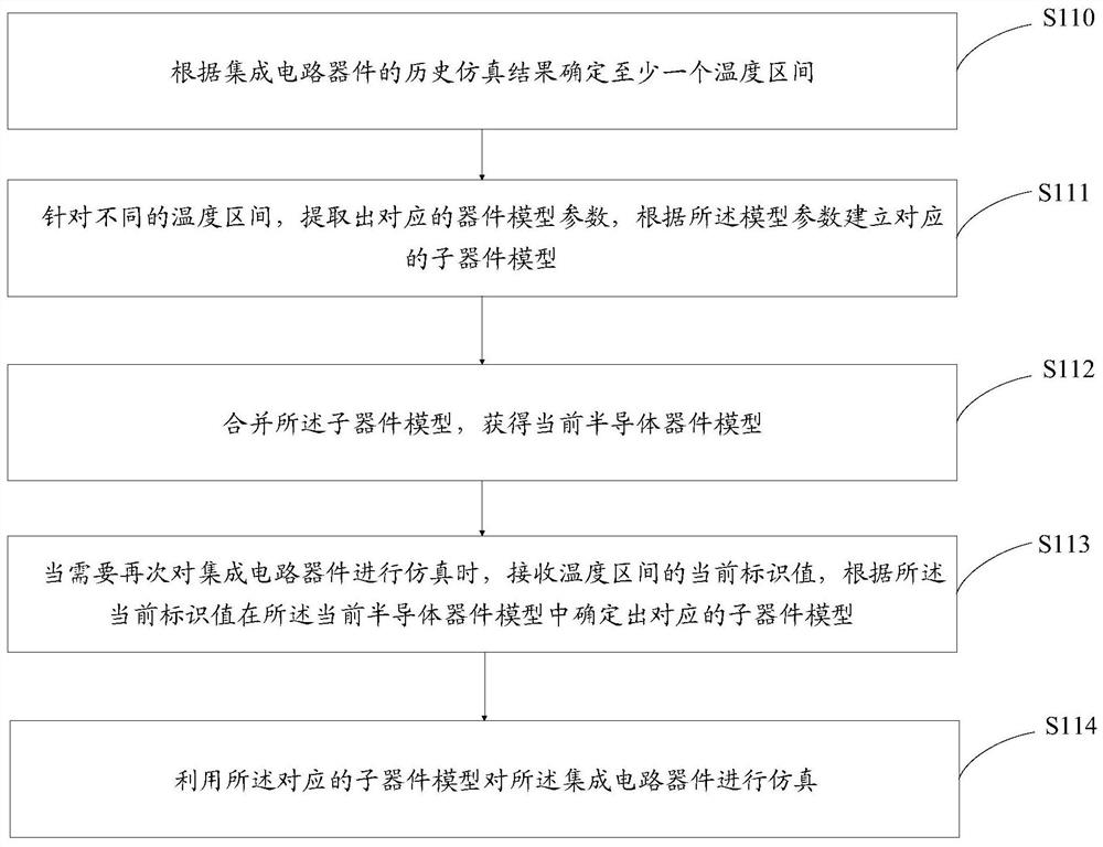
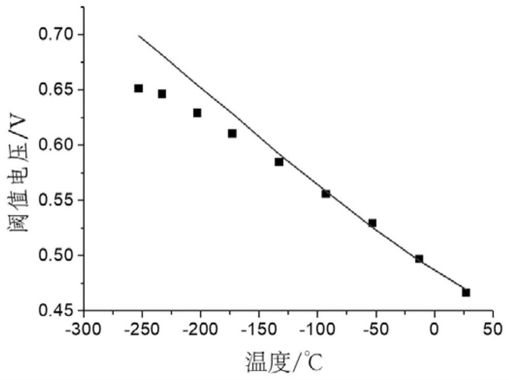
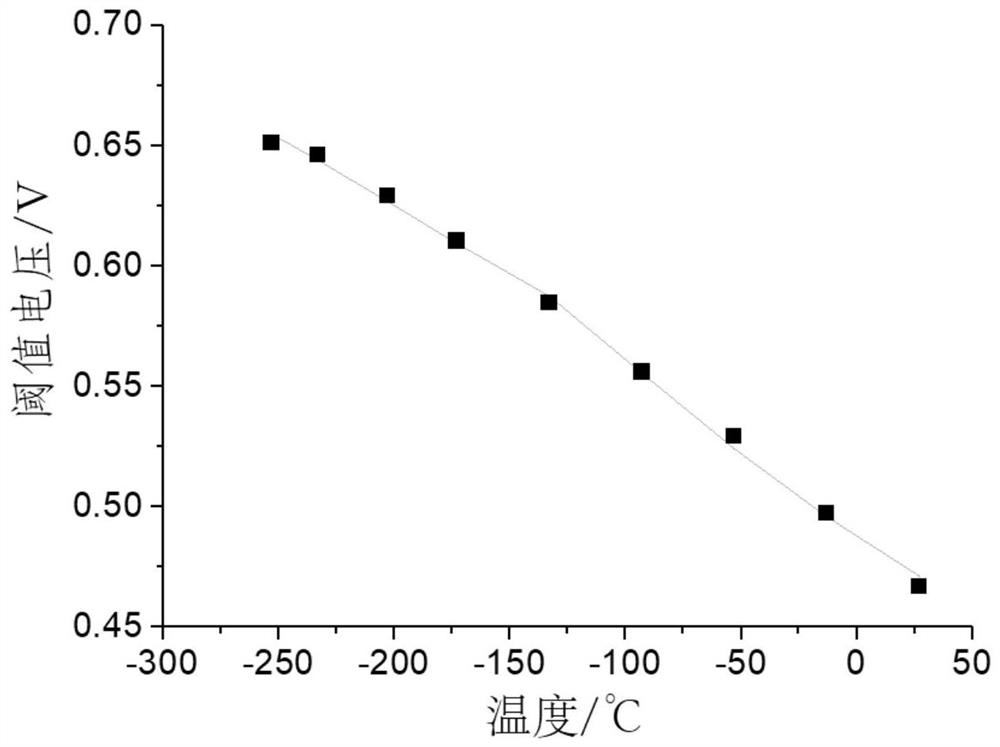
[0051] This embodiment provides a modeling method for a semiconductor device model, such as figure 1 As shown, the methods include:

[0052] S110. Determine at least one temperature range according to historical simulation results of integrated circuit devices;

[0053] When using a device model to simulate an integrated circuit device, it is mainly to simulate the performance test data of the integrated circuit device and obtain a simulation result, which can generally be presented as a curve. The historical simulation results described here are the simulation results obtained when the performance test data is simulated by using the historical semiconductor device model; the performance test data are the data required for simulating the integrated circuit device.

[0054] As an optional embodiment, at least one temperature range is determined according to historical simulation results of the device, including:

[0055] According to the fitting degree between the historical ...

Embodiment 2

[0122] This embodiment provides a modeling device for a semiconductor device model, such as Figure 4 As shown, the device includes: a first determining unit 41, an establishing unit 42, a combining unit 43, a second determining unit 44 and a simulation unit 45;

[0123] The first determination unit 41 is configured to determine at least one temperature range according to the historical simulation results of the integrated circuit device;

[0124]The establishment unit 42 is used to extract corresponding device model parameters for different temperature ranges, and establish corresponding sub-device models according to the model parameters;

[0125] A merging unit 43, configured to merge sub-device models to obtain a semiconductor device model;

[0126] The second determining unit 44 is configured to receive the current identification value of the temperature range when the integrated circuit device needs to be simulated again, and determine the corresponding sub-device model...


PUM


Abstract

The invention provides a modeling method and device for a semiconductor device model. The method comprises the steps of determining at least one temperature interval according to a historical simulation result of an integrated circuit device; for different temperature intervals, extracting corresponding device model parameters, and building corresponding sub-device models according to the model parameters; combining the sub-device models to obtain a current semiconductor device model; when the integrated circuit device needs to be simulated again, receiving a current identification value of atemperature interval, and determining a corresponding sub-device model in the current semiconductor device model according to the current identification value; simulating the integrated circuit deviceby using the corresponding sub-device model. Therefore, different temperature intervals correspond to different sub-device models, so that when the integrated circuit device is simulated, no matter what range the temperature is in, the suitable sub-device model can be used for simulating the integrated circuit device, the simulation precision is ensured, and the simulation requirement is met.

Description

technical field [0001] The invention belongs to the technical field of semiconductor device modeling, in particular to a modeling method and device for a semiconductor device model. Background technique [0002] With the development of integrated circuit technology and more and more widely used, the requirements of high reliability, high performance and low cost must be considered in the design of integrated circuits. . [0003] At present, the device model in the IC CAD simulation software is generally used to simulate and test the integrated circuit. In ICCAD software, the device model of MOSFET is the key link linking the design of integrated circuit devices and the function and performance of integrated circuit device products. With the size of integrated devices getting smaller and smaller, the scale of integration is getting bigger and bigger, and the process of integrated circuits is getting more and more complex, and the requirements for the accuracy of device mode...

Claims


Application Information

Patent Timeline
Patent Type & Authority Applications(China)
IPC IPC(8): G06F30/3308
CPCG06F30/3308
Inventor 卜建辉王成成李垌帅刘海南曾传滨韩郑生罗家俊
Owner INST OF MICROELECTRONICS CHINESE ACAD OF SCI
Why Eureka
Try Eureka