Bare chip KGD screening method based on adapter substrate

A screening method and bare chip technology, applied in the direction of electrical components, circuits, semiconductor/solid-state device testing/measurement, etc., can solve the unsuitable bare chip size, different PAD coordinates, small batch testing requirements, expensive fixtures, etc. problem, to achieve the effect of reducing test cost, reducing test cost, and reducing processing cost

Active Publication Date: 2020-09-22
XIAN MICROELECTRONICS TECH INST
View PDF17 Cites 6 Cited by
  • Summary
  • Abstract
  • Description
  • Claims
  • Application Information

AI Technical Summary

Problems solved by technology

[0004] The KGD test system represented by the above two devices has the problem of expensive test fixtures, which are only suitable for large-scale single-type bare chips, and are not suitable for the size of bare chips in MCM, different PAD coordinates and small batches. test requirements

Method used


Image

  • Bare chip KGD screening method based on adapter substrate
  • Bare chip KGD screening method based on adapter substrate
  • Bare chip KGD screening method based on adapter substrate

Examples


Embodiment Construction

[0028] The present invention will be further described in detail below in conjunction with specific embodiments, which are explanations of the present invention rather than limitations.

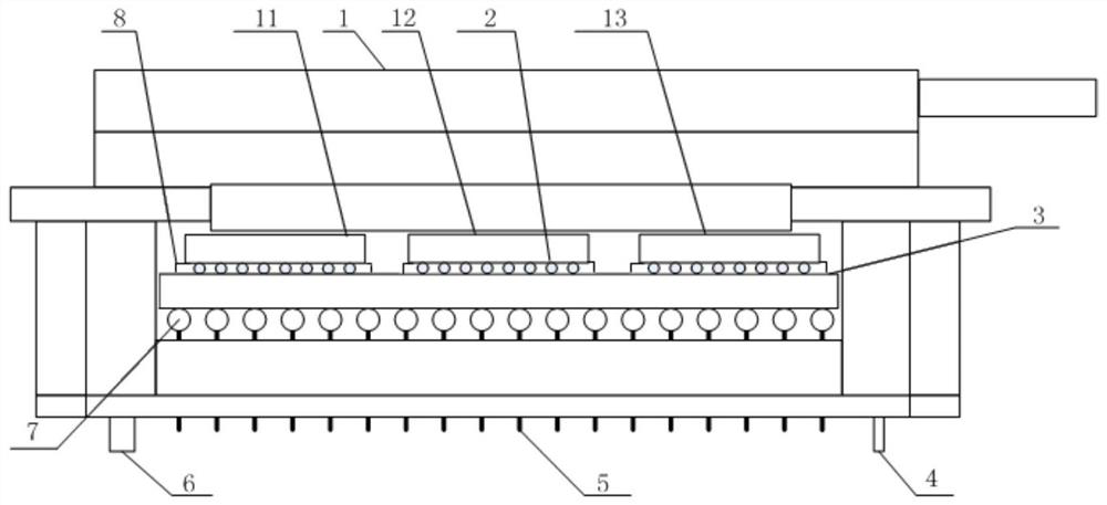
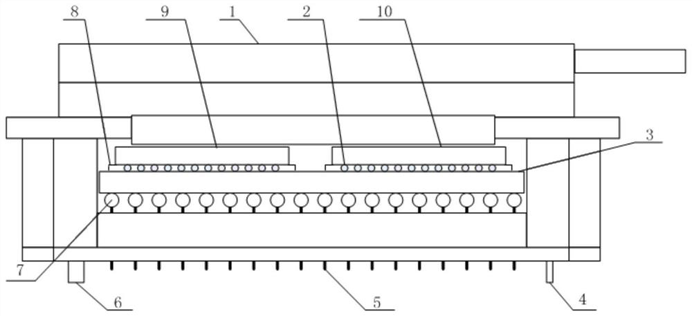
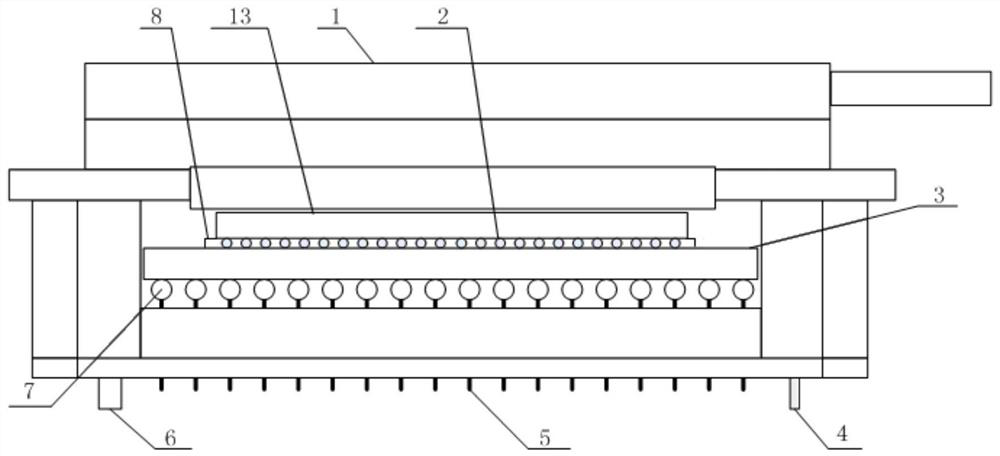
[0029] A kind of bare chip KGD screening method based on the transfer substrate of the present invention, such as Figure 4 and Figure 5 As shown, the specific steps are as follows:

[0030] Step 1, determine the bare chip standard component size,

[0031] Bare chip standard components can also be called silicon components, including silicon transfer substrates and bare chips. According to the size of silicon transfer standard substrates and bare chips, the number of bare chips of this size placed on silicon transfer substrates is determined to form each standard Bare chip components;

[0032] An example is as follows,

[0033] The area of ​​the silicon transfer substrate is 30mm×30mm, the diameter of the PAD at the bottom of the silicon transfer substrate is 200μm, and the spacing betwe...


PUM


Abstract

The invention discloses a bare chip KGD screening method based on an adapter substrate. The method comprises the steps of step 1, determining the number of FC bare chips which are placed on a siliconadapter standard substrate and of which the sizes to be measured; 2, sequentially preparing a TSV blind hole with the bottom filled with a conductive material, multilayer metal wiring and a bonding pad on the front surface of the silicon adapter standard substrate, thinning the back surface of the obtained silicon adapter standard substrate to expose the conductive material at the bottom of the TSV blind hole, and finally sequentially performing the multilayer metal wiring on the back surface and the bonding pad on the back surface; 3, inversely mounting the tested FC bare chips on the TSV silicon adapter standard substrate; and 4, filling a gap between the FC bare chips to be tested and the TSV silicon adapter standard substrate, then curing, and screening the obtained standard assembliesthrough a KGD test. According to the invention, one or more bare chips with different sizes and lead-out points with different physical distribution are converted into the standard sizes and standardlead-out points for arrangement, so that the test cost is reduced.

Description

technical field [0001] The invention relates to the technical field of bare chip KGD testing, in particular to a bare chip KGD screening method based on an adapter substrate. Background technique [0002] With the development of the semiconductor industry, the MCM packaging technology based on the bare chip has been paid more and more attention by the industry, but the packaging yield and reliability reduction caused by the unknown quality of the bare chip has greatly restricted the MCM packaging technology. Among them, the KGD test of the bare chip is the key to improving the yield and reliability of the MCM. [0003] The KGD process needs to install the chip in the fixture of the temporary carrier, complete the aging screening, and test the KGD. At present, many foreign semiconductor manufacturers have developed KGD technology, such as Texas Instruments (TI)'s Die Mate test system, Micro-ASI's Si-Star KGD test system, and AEHR's Die PAC. Micro-ASI's Si-Star test system c...

Claims


Application Information

Patent Timeline
Patent Type & Authority Applications(China)
IPC IPC(8): H01L21/66
CPCH01L22/14H01L22/30
Inventor 匡乃亮唐磊李宝霞赵超郭雁蓉
Owner XIAN MICROELECTRONICS TECH INST
Why Eureka
Try Eureka