Semiconductor structure and forming method thereof

A technology of semiconductor and stacked structure, which is applied in the direction of semiconductor devices, semiconductor/solid-state device manufacturing, electric solid-state devices, etc. It can solve the problems that the performance of 3D packaging structure needs to be improved, and achieve the effect of improving cutting accuracy and preventing damage

Pending Publication Date: 2020-09-22
CHANGXIN MEMORY TECH INC
View PDF0 Cites 1 Cited by
  • Summary
  • Abstract
  • Description
  • Claims
  • Application Information

AI Technical Summary

Problems solved by technology

[0004] However, the performance of the 3D packaging structure

Method used


Image

  • Semiconductor structure and forming method thereof
  • Semiconductor structure and forming method thereof
  • Semiconductor structure and forming method thereof

Examples


Embodiment Construction

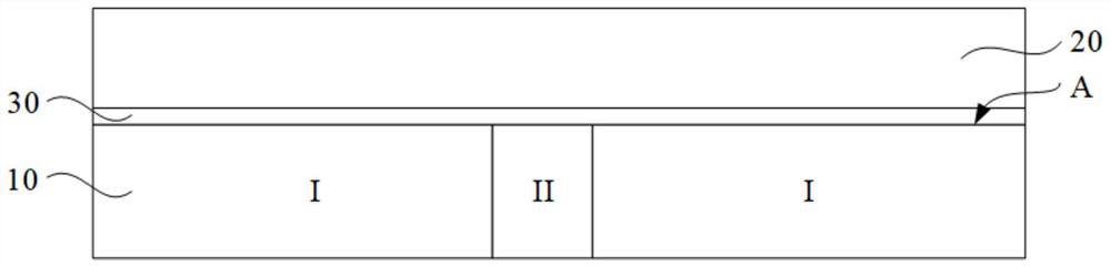
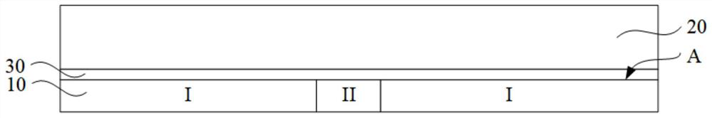
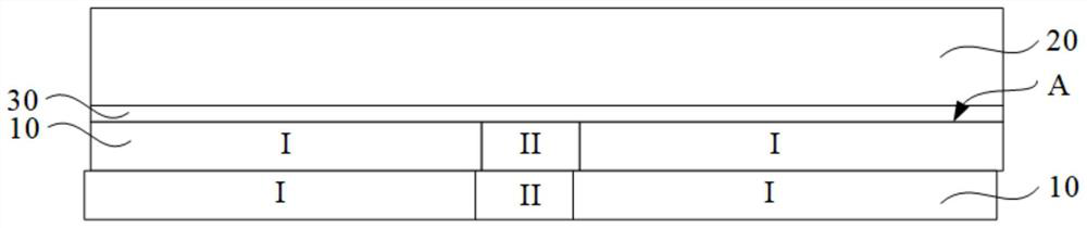
[0017] It can be seen from the background art that the performance of the existing 3D packaging structure needs to be improved.

[0018] The analysis found that with the increase in the number of stacked wafers in the 3D packaging structure, the thickness of the wafer stack structure is getting thicker and thicker. It is difficult to effectively cut the wafer stack structure with a single cutting process, and it is easy to cause mis-cutting of the chip.

[0019] In order to solve the above problems, an embodiment of the present invention provides a method for forming a semiconductor structure. The wafer stack structure is cut twice to complete the cutting of the wafer stack structure. Different, so as to avoid cutting to the chip by mistake during the cutting process, and prevent the chip from being damaged.

[0020] In order to make the purpose, technical solutions and advantages of the embodiments of the present invention clearer, the embodiments of the present invention wil...


PUM

PropertyMeasurementUnit
Widthaaaaaaaaaa
Widthaaaaaaaaaa

Abstract

The embodiment of the invention relates to a semiconductor structure and a forming method thereof. The forming method comprises the following steps: providing a wafer stacking structure to be cut; performing first cutting processing on the wafer stacking structure, forming a first through hole in the cutting channel, and extending the first through hole to form a first extending pattern in the direction perpendicular to the first surface and the extending direction of the cutting channel; performing second cutting treatment on the cutting channel at the bottom of the first through hole, cutting the wafer stacking structure until the wafer stacking structure is cut through; forming a second through hole in the cutting channel through second cutting treatment; in the direction perpendicularto the first face and the extending direction of the cutting channel, enabling the second through hole to extend to form a second extending pattern, wherein the second extending pattern and the firstextending pattern have an overlapping part, and the width of the overlapping part is less than the width of the first through hole and the width of the second through hole. According to the invention,the cutting of the wafer stacking structure can be effectively realized, and mistaken cutting of the chip is avoided.

Description

technical field [0001] Embodiments of the present invention relate to the field of semiconductor technology, and in particular to a semiconductor structure and a method for forming the same. Background technique [0002] In recent years, as semiconductor devices continue to respond to the demand for "faster, cheaper, and smaller", three-dimensional stacked 3D packaging technology has entered mainstream semiconductor manufacturing. Among them, TSV (Through Silicon Via) technology is interconnected through vertical chip vias, which brings shorter interconnection length and smaller packaging area, greatly improves signal transmission speed and reduces parasitic power consumption. [0003] The existing method for forming a three-dimensional stacked 3D packaging structure generally includes: stacking and bonding a plurality of wafers in a direction perpendicular to the surface of the wafer; after that, cutting the bonded plurality of wafers along a wafer dicing line , to obtain ...

Claims


Application Information

Patent Timeline
IPC IPC(8): H01L25/065H01L21/78H01L21/98
CPCH01L21/78H01L25/0657H01L25/50
Inventor 吴秉桓
Owner CHANGXIN MEMORY TECH INC
Why Eureka
Try Eureka