Supercharge Your Innovation With Domain-Expert AI Agents!

Semiconductor chip packaging structure and packaging part thereof

A technology of chip packaging structure and packaging components, applied in semiconductor/solid-state device manufacturing, electrical components, circuits, etc., can solve the problems of low paste efficiency and low degree of automation, achieve high paste efficiency, high degree of automation, and facilitate automatic paste Effect

Inactive Publication Date: 2020-10-02
顾骏
View PDF0 Cites 2 Cited by
  • Summary
  • Abstract
  • Description
  • Claims
  • Application Information

AI Technical Summary

Problems solved by technology

[0003] In the packaging process of semiconductor chips, it is necessary to paste the substrate and the wafer with glue. At present, most of them are pasted manually, with low degree of automation and low paste efficiency. Semiconductor chip packaging structure to overcome the deficiencies in current practical applications and meet current needs

Method used


Image

  • Semiconductor chip packaging structure and packaging part thereof
  • Semiconductor chip packaging structure and packaging part thereof
  • Semiconductor chip packaging structure and packaging part thereof

Examples


Embodiment 1

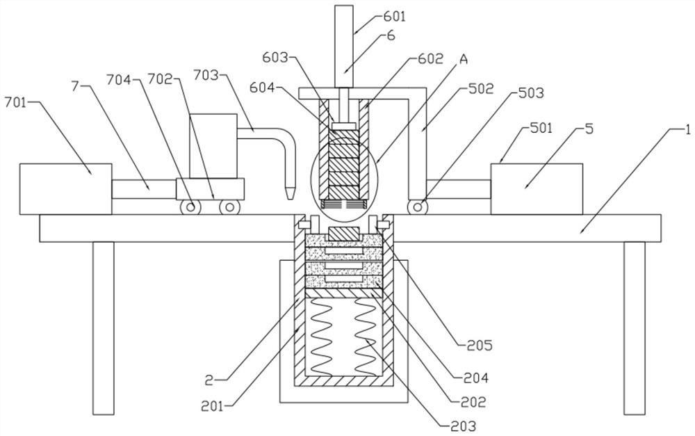
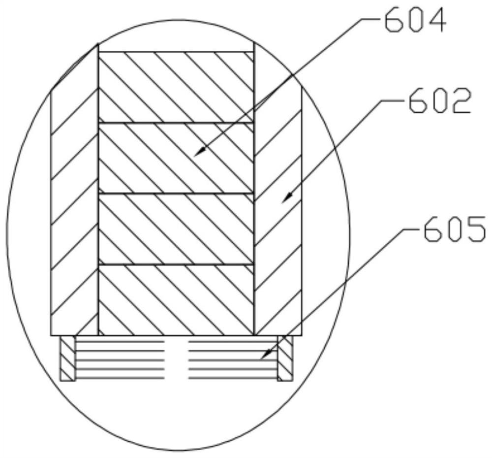
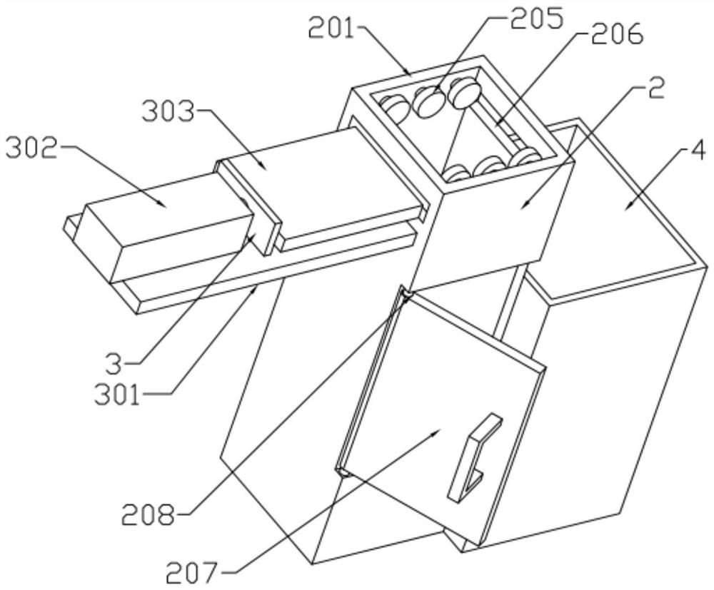
[0020] See Figure 1~3 In an embodiment of the present invention, a semiconductor chip packaging structure and its packaging components include a workbench 1, on which a substrate transport mechanism 2 is installed, and the substrate transport mechanism 2 includes: a storage shell 201, a support plate 202, a compression spring 203, a base plate 204, a limit roller 205, a discharge port 206, a cover plate 207 and a pin shaft 208, the storage shell 201 is connected to the workbench 1 by screws, and a support plate is installed in the storage shell 201 202. The support plate 202 is elastically connected to the inner bottom end of the storage case 201 through a plurality of compression springs 203. A plurality of substrates 204 are placed on the support plate 202. When the substrate 204 is placed on the support plate 202, the compression springs 203 is in a compressed state. A plurality of limit rollers 205 are installed on the left and right sides of the inner top of the storage s...

Embodiment 2

[0022] See Figure 1~3 In the embodiment of the present invention, the blanking mechanism 3 includes a mounting plate 301, a first cylinder 302, and a pushing block 303. The mounting plate 301 is mounted on the left side of the storage shell 201, and the mounting plate 301 is screwed It is detachably linked to the storage shell 201, the mounting plate 301 is equipped with a first air cylinder 302, and the telescopic rod of the first air cylinder 302 is connected to a pushing block 303, which is T-shaped.

[0023] For the semiconductor chip packaging structure and its packaging components, the cover 207 is first opened to place the substrate 204 on the support plate 202, and then the bottom plate 702 is driven by the third cylinder 701, and the dispenser 703 is driven onto the substrate 204 through the bottom plate 702. After dispensing, the third cylinder 701 drives the bottom plate 702 and the dispenser 703 to return, and the second cylinder 501 drives the L-shaped plate 502 to ...


PUM


Abstract

The invention discloses a semiconductor chip packaging structure and a packaging part thereof. The structure comprises a workbench; a base plate conveying mechanism is installed on the workbench; a discharging mechanism is installed on the left side of the base plate conveying mechanism; a material box is installed on the right side of the base plate conveying mechanism; a push-pull mechanism is installed on the right side of the base plate conveying mechanism and located at the top of the workbench; a wafer conveying mechanism is installed on the push-pull mechanism; and a dispensing device is installed on the left side of the base plate conveying mechanism and located at the top of the workbench. The structure is high in automation degree and high in pasting efficiency.

Description

Technical field [0001] The invention relates to the technical field of semiconductor chip production, in particular to a semiconductor chip packaging structure and packaging components thereof. Background technique [0002] Semiconductor packaging refers to the process of processing the tested wafers according to the product model and functional requirements to obtain independent chips. The packaging process is: the wafer from the previous wafer process is cut into small wafers after the dicing process, and then the cut wafers are attached to the corresponding islands of the substrate (lead frame) frame with glue, and then Use ultra-fine metal (gold, tin, copper, aluminum) wires or conductive resin to connect the bonding pads of the chip to the corresponding pins of the substrate to form the required circuit; then the independent chip is packaged and protected with a plastic casing. [0003] In the semiconductor chip packaging process, it is necessary to paste the substrate and th...

Claims


Application Information

Patent Timeline
IPC IPC(8): H01L21/67
CPCH01L21/67011H01L21/67121
Inventor 顾骏
Owner 顾骏
Features
  • R&D
  • Intellectual Property
  • Life Sciences
  • Materials
  • Tech Scout
  • Unparalleled Data Quality
  • Higher Quality Content
  • 60% Fewer Hallucinations
Learn More