Chip assembly bonding module, clamp and chip assembly clamping method

A module and bonding technology, applied in the manufacturing of electrical components, laser parts, semiconductor/solid-state devices, etc., can solve problems such as difficulty in clamping chip components, and achieve the effect of reducing the probability of damage

Pending Publication Date: 2020-10-09
GUANGXUN SCI & TECH WUHAN
View PDF4 Cites 0 Cited by
  • Summary
  • Abstract
  • Description
  • Claims
  • Application Information

AI Technical Summary

Problems solved by technology

[0004] In view of this, the embodiment of the present application expects to provide a chip component bonding module, a jig a

Method used


Image

  • Chip assembly bonding module, clamp and chip assembly clamping method
  • Chip assembly bonding module, clamp and chip assembly clamping method
  • Chip assembly bonding module, clamp and chip assembly clamping method

Examples


Embodiment Construction

[0050] It should be noted that, in the case of no conflict, the embodiments in the application and the technical features in the embodiments can be combined with each other. Undue Limitation of This Application.

[0051] The orientation terms in the description of the application are only for the convenience of describing the application and simplifying the description, rather than indicating or implying that the device or element referred to must have a specific orientation, be constructed and operated in a specific orientation, and therefore cannot be construed as a reference to this application. Application Restrictions.

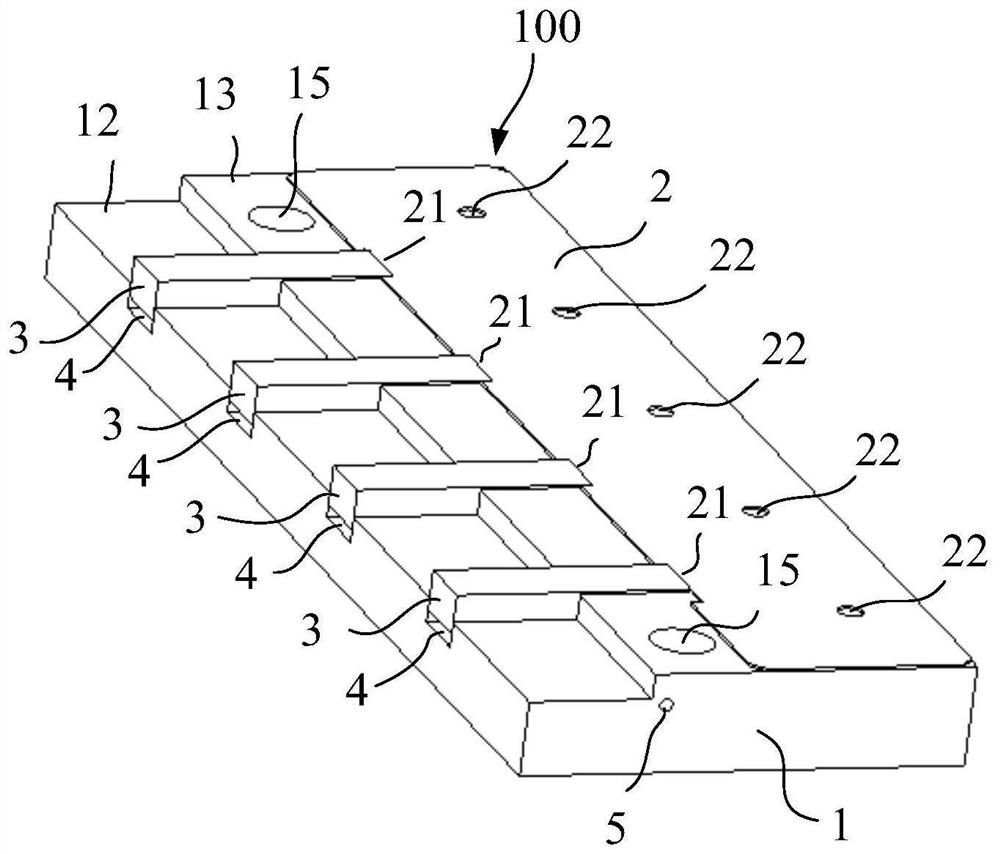
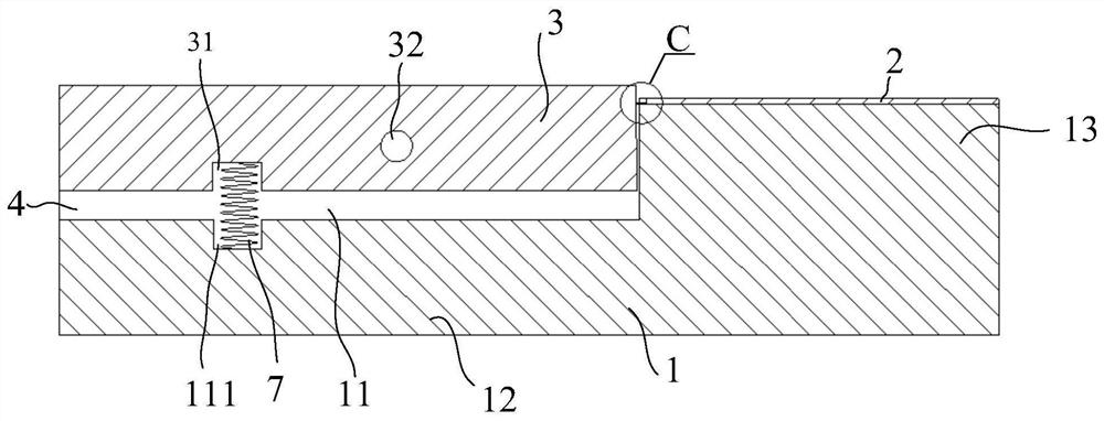
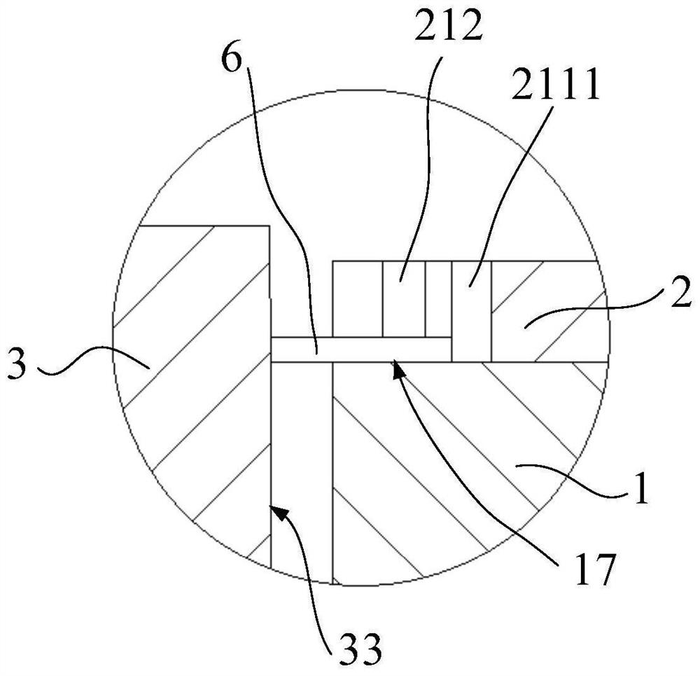
[0052] In the field of optical communication R&D and manufacturing, for active optical devices such as optical transmitters, four chips are usually eutectic onto ceramic substrates, and then bonded together on tungsten-copper components for aging. During the aging process, if there is a problem with one chip, the rest of the chips will be scrapped and it...


PUM


Abstract

The invention provides a chip assembly bonding module, a clamp and a chip assembly clamping method which are used for clamping a chip assembly in a gold wire bonding process. The bonding module comprises a module body, a clamping piece, an elastic piece and a limiting piece. A positioning surface is formed on the module body, and the clamping piece is movably arranged on the module body. The elastic piece is connected with the module body and the clamping piece, and when the elastic piece is in an initial state, the bottom height of the end, close to the limiting piece, of the clamping piece is equal to or lower than the positioning face. The limiting piece is arranged on the module body. A positioning area for containing the chip assembly is formed between the clamping piece and the limiting piece, the positioning face is located in the positioning area to support the chip assembly, and the elastic piece is used for enabling the clamping piece to apply clamping force to the chip assembly. According to the bonding module of the chip assembly provided by the invention, the chip assembly is stably clamped between the clamping piece and the limiting piece through the elastic piece, sothat the probability that the chip assembly is damaged in a gold wire bonding process is effectively reduced.

Description

technical field [0001] The present application relates to the field of gold wire bonding of chips, in particular to a bonding module of a chip component, a fixture and a clamping method of a chip component. Background technique [0002] In the gold wire bonding process of a single chip, it is sometimes necessary to perform gold wire bonding on a single chip. At this time, a single chip, such as an LD single chip laser, needs to be eutectically welded on a ceramic substrate to form a chip assembly. During the gold wire bonding process of the chip component, it needs to be clamped by a fixture to prevent bonding failure. [0003] However, the size of chip components is usually very small, the length, width and height are only a few tenths of a millimeter, and they are very easy to be damaged and dirty, and their clamping in the gold wire bonding process is very difficult. Contents of the invention [0004] In view of this, the embodiment of the present application expects t...

Claims


Application Information

Patent Timeline
IPC IPC(8): H01L21/67H01L21/683H01L21/687H01S5/022
CPCH01L21/67138H01L21/6838H01L21/68728
Inventor 杨适张博
Owner GUANGXUN SCI & TECH WUHAN
Why Eureka
Try Eureka