
Protection ring for improving negative current latch-up prevention capability of high-voltage integrated circuit and implementation method thereof

A technology of high-voltage integrated circuits and guard rings, which is applied to circuits, electrical components, and electric solid-state devices, and can solve problems such as reducing the NPN current gain of parasitic triodes, reducing voltage, and reducing

Active Publication Date: 2020-10-20
SHANGHAI HUALI MICROELECTRONICS CORP
View PDF12 Cites 1 Cited by
  • Summary
  • Abstract
  • Description
  • Claims
  • Application Information

AI Technical Summary

Problems solved by technology

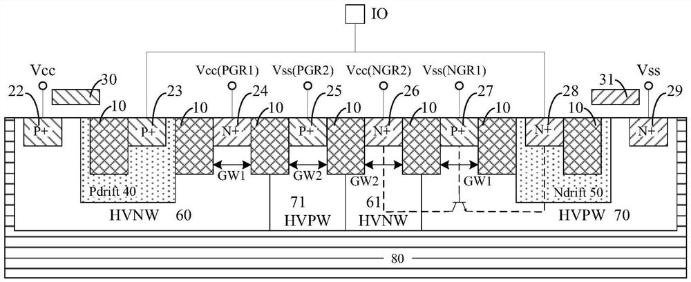
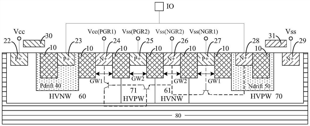
[0011] In order to reduce the width of the inner guard ring around the high-voltage device to achieve the purpose of saving layout area, the industry proposes as follows: image 3 In the new high-voltage integrated circuit guard ring structure shown, the outer guard ring of the high-voltage NLDMOS in the IO circuit is doped with a high concentration of N-type (N+) 26, that is, NGR2 is grounded to Vss instead of the power supply Vcc. The advantage of this approach is to reduce Reduce the voltage of the collector of the parasitic NPN transistor (high concentration N-type doping (N+) 28, namely NLDMOS Drain / HVPW70 / NGR2), reduce the probability of the parasitic NPN transistor being triggered, but increase the positive current at the high-voltage IO terminal The risk of impact mode latch-up, which is due to the parasitic transistor NPN (HVNW 60 / HVPW 71 / NGR2) The current gain (β) is too large
[0012] The industry then proceeds in such image 3 Based on the existing high-voltage integrated circuit guard ring structure 1, the proposed Figure 4 The existing high-voltage integrated circuit guard ring structure shown, which will image 3 The high-concentration N-type doping (N+) 26 in the outer guard ring of the NLDMOS of the existing high-voltage integrated circuit guard ring structure is removed to form a Schottky junction (Schottky diode), because the Schottky junction is a metal electrode and the second The high-voltage N well 61 is in direct contact with the structure, which reduces the efficiency of electrons entering the second high-voltage P well 71 from the electrode 26, that is, reduces the current gain ( β), which reduces the risk of positive current surge mode latch-up at the high-voltage IO terminal, but this method is easy to cause interface defects due to the introduction of Schottky junctions, and also increases process complexity.

Method used


Image

  • Protection ring for improving negative current latch-up prevention capability of high-voltage integrated circuit and implementation method thereof
  • Protection ring for improving negative current latch-up prevention capability of high-voltage integrated circuit and implementation method thereof
  • Protection ring for improving negative current latch-up prevention capability of high-voltage integrated circuit and implementation method thereof

Examples


Embodiment Construction

[0044] The implementation of the present invention is described below through specific examples and in conjunction with the accompanying drawings, and those skilled in the art can easily understand other advantages and effects of the present invention from the content disclosed in this specification. The present invention can also be implemented or applied through other different specific examples, and various modifications and changes can be made to the details in this specification based on different viewpoints and applications without departing from the spirit of the present invention.

[0045] Figure 5 It is a circuit structure diagram of a protection ring for improving the anti-negative current latch-up capability of a high-voltage integrated circuit according to the present invention. Such as Figure 5 As shown, the present invention is a protection ring for improving the anti-negative current latch-up ability of high-voltage integrated circuits, including: a plurality...


PUM


Abstract

The invention discloses a protection ring for improving the negative current latch-up prevention capability of a high-voltage integrated circuit and an implementation method thereof. According to theinvention, a high-concentration N type dopant (26) of an outer protection ring of an existing high-voltage NLDMOS is connected in series with a non-metal silicified polycrystalline silicon resistor and then is connected to a power supply terminal Vcc; once a parasitic NPN triode is mistakenly triggered, the voltage of the parasitic NPN triode falls on the collector electrode of the parasitic NPN triode can be reduced. Therefore, the parasitic NPN triode is prevented from entering a conduction maintaining state after being mistakenly triggered, the latch-up capability of the negative current impact preventing mode of the high-voltage IO terminal is improved, the width of a protection ring in the high-voltage device NLDMOS is reduced, and the layout area is saved.

Description

technical field [0001] The invention relates to the field of integrated circuit design, in particular to a protection ring for improving the anti-negative current latch-up capability of a high-voltage integrated circuit and an implementation method thereof. Background technique [0002] The double guard ring structure is used in IO circuits of almost all integrated circuit process platforms to enhance the anti-latch capability of integrated circuits. However, in high-voltage integrated circuits, even if the double-protection structure is applied, failures often occur due to insufficient anti-latch-up capability of the high-voltage IO terminal anti-negative current impact mode. After failure analysis, it is found that the cause of failure is often NLDMOS in the high-voltage integrated circuit IO circuit. (The following is for the convenience of expression, the high-voltage device is taken as an example of LDMOS) drain, and its high-voltage P-well and the outer guard ring (NGR...

Claims


Application Information

Patent Timeline
IPC IPC(8): H01L27/02
CPCH01L27/0296H01L27/0288
Inventor 朱天志黄冠群陈昊瑜邵华
Owner SHANGHAI HUALI MICROELECTRONICS CORP
Learn More