Latch-preventing N type silicon on insulator transverse isolated gate bipolar transistor

A bipolar transistor and silicon-on-insulator technology, which is applied in semiconductor devices, electrical components, circuits, etc., can solve problems such as increased device area, increased process version complexity, and reduced current capability, and achieves the risk of latch failure Effects of reducing and improving current conduction capability and reducing power consumption

Active Publication Date: 2012-10-31
SOUTHEAST UNIV
View PDF3 Cites 7 Cited by
  • Summary
  • Abstract
  • Description
  • Claims
  • Application Information

AI Technical Summary

Problems solved by technology

There are many similar methods, and they also have shortcomings under the condition of improving the latch-up problem, such as the decrease of current capability, the significant increase of device area, and the increase of complexity of process version, etc.

Method used


Image

  • Latch-preventing N type silicon on insulator transverse isolated gate bipolar transistor
  • Latch-preventing N type silicon on insulator transverse isolated gate bipolar transistor
  • Latch-preventing N type silicon on insulator transverse isolated gate bipolar transistor

Examples


Embodiment Construction

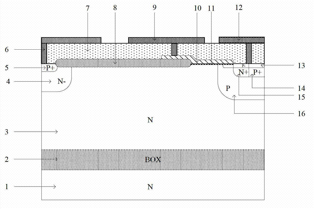
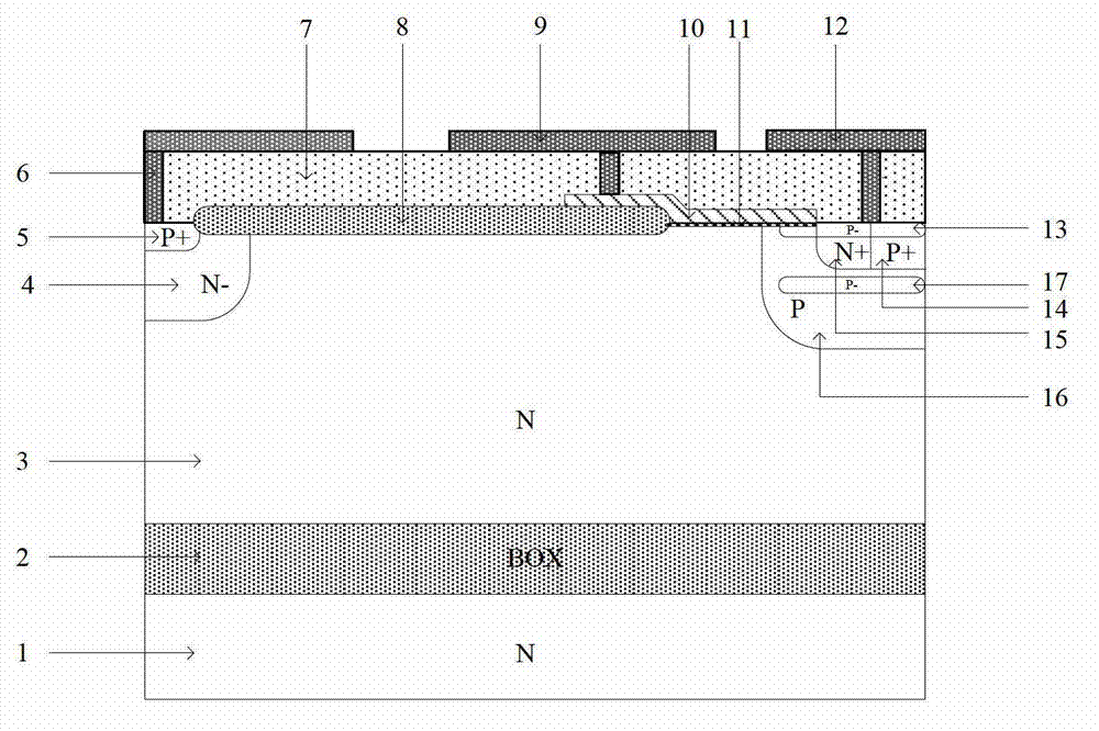
[0017] Attached below figure 2 , the present invention is described in detail, a kind of anti-latch-up N-type silicon-on-insulator lateral insulated gate bipolar transistor, comprising: N-type substrate 1, buried oxygen 2 is arranged on N-type substrate 1, buried oxygen 2 N-type epitaxial layer 3 is arranged on it, N-type buffer well 4 and P-type body region 16 are arranged inside N-type epitaxial layer 3, P-type anode region 5 is arranged in N-type buffer well 4, P-type body An N-type negative region 15 and a P-type body contact region 14 are arranged in the region 16, and a gate oxide layer 11 and a field oxide layer 8 are arranged on the surface of the N-type epitaxial layer 3, and one end of the gate oxide layer 11 and the end of the field oxide layer 8 The other end of the gate oxide layer 11 extends to the N-type negative region 15 and ends at the N-type negative region 15, and the other end of the field oxide layer 8 extends to the P-type positive region 5 and ends at ...


PUM


Abstract

The invention discloses a latch-preventing N type silicon on insulator transverse isolated gate bipolar transistor which comprises an N type substrate, wherein the N type substrate is provided with buried oxide, the buried oxide is provided with an N type epitaxial layer, and the N type epitaxial layer is internally provided with an N type buffering trap and a P type body region; the N type buffering trap is internally provided with a P type positive region, the P type positive region is provided with an N type negative region and a P type body contact region, and the surface of the N type epitaxial layer is provided with a gate oxide layer and a field oxide layer; and the surfaces of the N type negative region and the P type body contact region are provided with shallow P type trap regions, the surface of the gate oxide layer is provided with a polysilicon gate, and the surfaces of the field oxide layer, the P type body contact region, the N type negative region, the polysilicon gate and the P type positive region are provided with a passivation layer respectively. The transverse isolated gate bipolar transistor is characterized in that the positive inferior of the shallow P type trap region is also provided with a deep P type trap region is arranged under the shallow P type trap region, which shares one photoetching plate together with the shallow P type trap region and is formed by injection of high energy ions; and the deep P type trap region effectively reduces the conduction resistor of a body region, the current capacity of a device is improved, and meanwhile, and the risk of the latch generated in a working process is reduced.

Description

technical field [0001] The invention mainly relates to the field of high-voltage power semiconductor devices, specifically, an N-type silicon-on-insulator lateral insulated gate bipolar transistor with strong anti-latch capability, which is suitable for plasma flat panel display equipment, half-bridge drive circuits and Driver chips in the field of automobile production. Background technique [0002] Today, high voltage integrated circuits are one of the fastest growing power semiconductor industries. In this situation, the Silicon On Insulator (SOI) process technology came out. Its unique insulating buried layer completely isolates the device from the substrate, which greatly reduces the parasitic effect of the silicon device and greatly improves the performance of the silicon device. Device and circuit performance. Silicon-on-insulator lateral insulated gate bipolar transistor (SOI-LIGBT) is a typical device based on SOI technology, which has the advantages of high withs...

Claims


Application Information

Patent Timeline
Patent Type & Authority Applications(China)
IPC IPC(8): H01L29/739H01L29/06
Inventor 刘斯扬唐正华潘红伟钱钦松孙伟锋陆生礼时龙兴
Owner SOUTHEAST UNIV
Why Eureka
Try Eureka