Super junction MOSFET with reverse conductive trench gate structure

A reverse conduction, trench gate technology, applied in circuits, electrical components, semiconductor devices, etc., can solve problems such as increasing resistance and reducing reverse recovery speed

Active Publication Date: 2020-10-20
SICHUAN UNIV
View PDF10 Cites 5 Cited by
  • Summary
  • Abstract
  • Description
  • Claims
  • Application Information

AI Technical Summary

Problems solved by technology

Of course, this will increase the resistance and reduce the reverse recovery speed to a certain extent

Method used


Image

  • Super junction MOSFET with reverse conductive trench gate structure
  • Super junction MOSFET with reverse conductive trench gate structure
  • Super junction MOSFET with reverse conductive trench gate structure

Examples


Embodiment Construction

[0024] The present invention will be described in detail below in conjunction with the accompanying drawings.

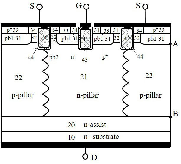
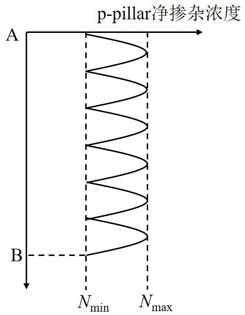
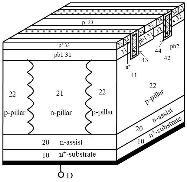
[0025] figure 1 It is a trench gate super junction MOSFET of the present invention. figure 1 The main difference between the structure and the ordinary super junction MOSFET is that the doping concentration of the p-pillar region (p-pillar region 22) is non-uniformly doped, and the slot-shaped gate structure for reverse conduction (made of insulating dielectric layer 44 and conductive material 42). figure 1 There are two main advantages of the structure: first, the reverse recovery charge of the body diode is low; second, the current and voltage oscillations during the reverse recovery process are small. These two advantages are explained separately below.

[0026]During reverse conduction, the potential of the gate G relative to the source S is 0 or a negative value, and the slot-type gate structure (composed of insulating dielectric layer 43 and conductive mater...


PUM

PropertyMeasurementUnit
thicknessaaaaaaaaaa
thicknessaaaaaaaaaa

Abstract

The invention provides a super junction MOSFET (Metal-Oxide-Semiconductor Field Effect Transistor) device. Non-uniform doping is adopted in a semiconductor region of a second conductive type in a voltage-withstanding layer to improve the resistance of the region, and a reverse conductive groove type gate structure is introduced to reduce the hole injection efficiency of the body diode. A conductormaterial leading-out end in the groove type gate structure used for reverse conduction is a source electrode of the device, the side face of the conductor material leading-out end is in direct contact with a source region and a lightly-doped base region of the second conductive type, and the bottom of the conductor material leading-out end is in direct contact with the voltage-withstanding layer.Compared with a traditional super junction MOSFET device, the super junction MOSFET device provided by the invention has a more excellent body diode reverse recovery characteristic.

Description

technical field [0001] The invention belongs to semiconductor devices, especially semiconductor power devices. Background technique [0002] Superjunction Metal-Oxide-Semiconductor Field Effect Transistor (Superjunction Metal-Oxide-Semiconductor Field Effect Transistor, Superjunction MOSFET) is a low conduction power switching device with a voltage range of 400 V to 1200 V. widely used. A voltage-resistant layer structure in which n-columns / p-columns are alternately arranged is adopted in the super-junction MOSFET. When the effective doping concentrations of the n-column and the p-column are equal or close to the same, the electric field distribution in the withstand voltage layer as a whole will show the situation of an undoped semiconductor, that is, the electric field slope is zero. This enables the n-column region and the p-column region to obtain a higher breakdown voltage in the case of a higher doping concentration, and obtain an excellent trade-off relationship bet...

Claims


Application Information

Patent Timeline
Patent Type & Authority Applications(China)
IPC IPC(8): H01L29/78H01L29/06
CPCH01L29/0634H01L29/7804H01L29/7813
Inventor 黄铭敏李睿李芸
Owner SICHUAN UNIV
Why Eureka
Try Eureka