A kind of superjunction mosfet device and its manufacturing method

A manufacturing method and device technology, applied in semiconductor/solid-state device manufacturing, semiconductor devices, electrical components, etc., can solve problems affecting device reliability, increase circuit power consumption, increase device leakage, etc., and increase manufacturing costs and process difficulties. Effect

Active Publication Date: 2016-06-08
WUXI NCE POWER
View PDF6 Cites 0 Cited by
  • Summary
  • Abstract
  • Description
  • Claims
  • Application Information

AI Technical Summary

Problems solved by technology

Due to the poor reverse recovery characteristics of ordinary super-junction MOSFET devices T2 and T3, diodes D4 and D5 are respectively connected in parallel on T2 and T3, although this can solve the problem of T2 and T3 easily due to excessively high Irrm However, due to the addition of additional devices in the circuit, the power consumption of the entire circuit will also increase, and the efficacy of T2 and T3 will also decrease. This situation is constantly pursuing energy saving and consumption reduction. Under the direction of development, it is not a good choice
[0004] In order to solve the problem of reverse recovery characteristics of the body diode of super-junction MOSFET devices, three methods have been proposed or adopted at present: 1. Use electron irradiation to create defects in the drift layer, reduce the carrier lifetime d

Method used


Image

  • A kind of superjunction mosfet device and its manufacturing method
  • A kind of superjunction mosfet device and its manufacturing method
  • A kind of superjunction mosfet device and its manufacturing method

Examples


Embodiment Construction

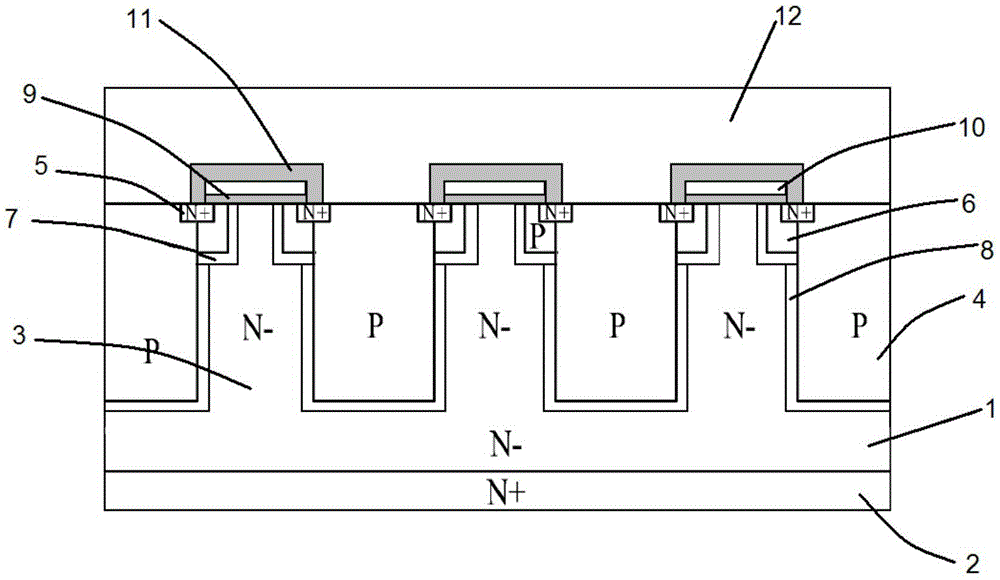
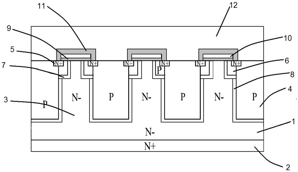
[0056] The specific embodiments of the present invention will be further described below in conjunction with the drawings.

[0057] Such as image 3 As shown, taking an N-type super junction MOSFET device as an example, on the cross-section of the MOSFET device, the semiconductor substrate includes an N-type drift layer 1 and an N+ type substrate 2 located below the N-type drift layer 1. The N+ type substrate 2 Adjacent to the N-type drift layer 1, the concentration of the N+ type substrate 2 is greater than that of the N-type drift layer 1.

[0058] On the cross section of the MOSFET device, the N-type drift layer 1 includes a plurality of pairs of first pillars with N-type conductivity and second pillars with P-type conductivity, that is, N-type pillars 3 form a first The P-type pillar 4 forms the second pillar. The N-type pillars 3 and the P-type pillars 4 are alternately arranged in the N-type drift layer 1 to form a super junction structure. The N-type pillar 3 and the P-typ...


PUM


Abstract

The invention discloses a super junction MOSFET device and a manufacturing method thereof. A first buffer layer of the first conductivity type adjacent to the body region of the second conductivity type and a second column of the second conductivity type are arranged in the drift layer of the first conductivity type. The second buffer layer of the first conductivity type; the body region of the second conductivity type and the drift layer of the first conductivity type are separated by the first buffer layer of the first conductivity type, and the second column of the second conductivity type is separated from the second column of the first conductivity type. A pillar is isolated by the second buffer layer of the first conductivity type; the impurity concentration of the first buffer layer of the first conductivity type and the second buffer layer of the first conductivity type is greater than that of the first conductivity type drift layer and the first conductivity type The impurity concentration of the first column. The invention has more optimized body diode reverse recovery characteristics, simple process, is compatible with the existing super junction MOSFET manufacturing process, and is suitable for mass production requirements.

Description

Technical field [0001] The invention relates to a semiconductor device and a manufacturing method thereof, in particular to a semiconductor device with a super junction structure and a manufacturing method thereof. Background technique [0002] In the field of medium and high voltage power semiconductor devices, the super junction structure (SuperJunction) has been widely adopted. Such as figure 1 As shown, in the drift region of the power MOSFET, a plurality of P-N column pairs formed by alternately adjacently arranged N columns and P columns form a super junction structure. When the MOSFET device with a super junction structure is turned off, the N pillars and P pillars in the super junction structure are respectively depleted, and the depletion layer extends from the PN junction interface between each N pillar and the P pillar. The mass is equal to the amount of impurities in the P column, so the depletion layer extends and completely depletes the N column and the P column, t...

Claims


Application Information

Patent Timeline
IPC IPC(8): H01L29/78H01L29/06H01L21/336
Inventor 朱袁正李宗清
Owner WUXI NCE POWER
Why Eureka
Try Eureka