High Power Light Emitting Diode Package

a light-emitting diode and high-power technology, applied in the field of high-power led packages, can solve the problems of low heat-releasing performance, large heat generation, and inconvenient coupling method described above, and achieve the effect of high-power led and efficient coupling

Inactive Publication Date: 2008-04-17
ALTI ELECTRONICS
View PDF6 Cites 80 Cited by
  • Summary
  • Abstract
  • Description
  • Claims
  • Application Information

AI Technical Summary

Benefits of technology

[0015]It is an object of the present invention to provide a high power LED package in which the heat sink, the lead frames and the housing can be efficiently coupled without cutting the heat sink nor using a discrete coupling means such as the ties.

Problems solved by technology

The LED generates lots of heat since it can not transform an electric current into light 100%.
However, the coupling method described above is not suitable for mass production because an insertion location may change according to the insertion strength and the housing 10 may easily be transformed.
In addition, a step difference between the lead frame 20 and the bottom of the heat sink 30 may occur when the LED package is mounted on a printed circuit board (“PCB”) by using a surface-mount technology (“SMT”), so that the bottom of the heat sink 30 is not closely mounted on the PCB, leading to a low heat releasing performance.
Also, in the coupling method using the ties 70, the step portion and the groove 35 should be formed in the heat sink 30 by using a cutting technique, and so the precise assembly is required, leading to the high manufacturing cost.

Method used


Image

  • High Power Light Emitting Diode Package
  • High Power Light Emitting Diode Package
  • High Power Light Emitting Diode Package

Examples


Embodiment Construction

[0050]Reference will now be made in detail to the embodiments of the present invention, examples of which are illustrated in the accompanying drawings, wherein like reference numerals refer to the like elements throughout. The embodiments are described below in order to explain the present invention by referring to the figures.

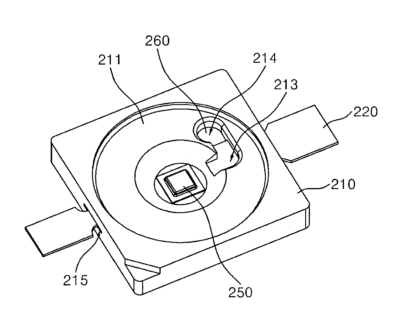
[0051]FIG. 6 is a perspective view illustrating a high power LED package in which a lens is removed according to a first exemplary embodiment of the present invention. FIG. 7 is a cross-sectional view taken along line B-B′ of FIG. 6. FIG. 8 is a perspective view illustrating the high power LED package according to the first embodiment of the present invention, which is shown from a bottom. FIG. 9 is a partial exploded perspective view illustrating the high power LED package of FIG. 6. FIG. 10 is a partial exploded perspective view illustrating the high power LED package of FIG. 9, which is shown from a bottom.

[0052]The high power LED package according to the f...


PUM


Abstract

A high power light emitting diode (“LED”) package is disclosed. The high power LED package includes a housing made of an insulating material and having a cavity in its central portion; a lead frame made of a conductive material, including an inner lead exposed by the cavity of the housing and an outer lead extending outside the housing; a heat sink above which the inner lead is placed and having a portion exposed by the cavity of the housing; an LED chip mounted on the exposed portion of the heat sink and electrically connected to the inner lead; a lens portion coupled to the housing to cover the cavity of the housing; and an insulating adhesive sheet interposed between the inner lead and the heat sink for electrically insulating and thermally coupling the inner lead and the heat sink.

Description

CROSS-REFERENCE TO RELATED APPLICATION[0001]This application claims priority to and the benefit of Korean Patent Application No. 2006-98861, filed Oct. 11, 2006, the disclosure of which is incorporated herein by reference in its entirety.BACKGROUND OF THE INVENTION[0002]1. Field of the Invention[0003]The present invention relates to a light emitting diode (“LED”) package and, more particularly, to a high power LED package.[0004]2. Description of the Related Art[0005]An LED is a semiconductor which emits light of various colors when an electric current is applied thereto. A color of light emitted from the LED depends on a chemical component which constitutes the LED, and the LED is increasingly in demand due to advantages such as a long lifespan, low power consumption, and an excellent initial driving characteristic. The LED generates lots of heat since it can not transform an electric current into light 100%. Components of the LED get stress due to a difference between their thermal...

Claims


Application Information

Patent Timeline
Patent Type & Authority Applications(United States)
IPC IPC(8): F21V29/00H01L33/44H01L33/50H01L33/58H01L33/60H01L33/62
CPCH01L33/62H01L33/642H01L33/647H01L2224/48091H01L2224/48247H01L2924/00014
Inventor KIM, DONG-SELKIM, DONG SOO
Owner ALTI ELECTRONICS
Why Eureka
Try Eureka