Shielded gate field effect transistor, method for forming same, and semiconductor device

A field-effect transistor and shielded gate technology, applied in semiconductor devices, semiconductor/solid-state device manufacturing, electrical components, etc., can solve problems such as uneven etching, affecting the shape of shielding electrodes, etc., to improve stability and reduce manufacturing difficulty. , the effect of ensuring performance stability

Active Publication Date: 2020-12-25
SEMICON MFG ELECTRONICS (SHAOXING) CORP +1
View PDF4 Cites 0 Cited by
  • Summary
  • Abstract
  • Description
  • Claims
  • Application Information

AI Technical Summary

Problems solved by technology

[0005] The object of the present invention is to provide a method for forming a shielded gate field effect transistor, so as to solve the problem of uneven etching caused by the existence of gaps in the preparation process of the shielded electrode, which affects the morphology of the shielded electrode.

Method used


Image

  • Shielded gate field effect transistor, method for forming same, and semiconductor device
  • Shielded gate field effect transistor, method for forming same, and semiconductor device
  • Shielded gate field effect transistor, method for forming same, and semiconductor device

Examples


Embodiment Construction

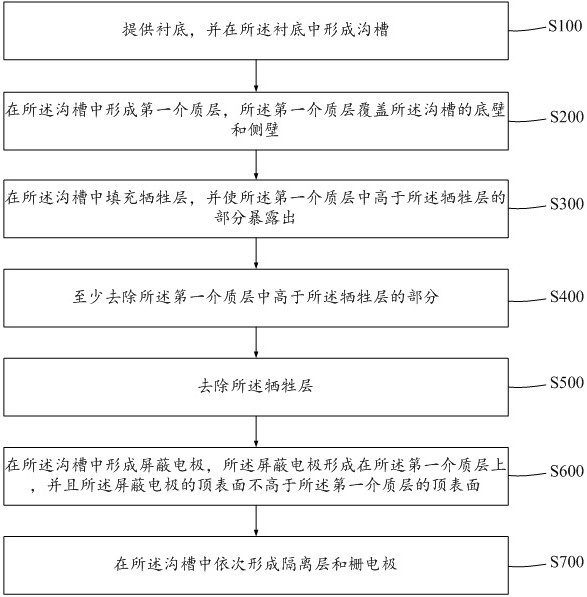
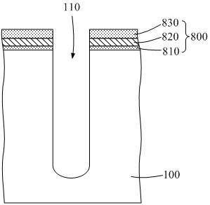
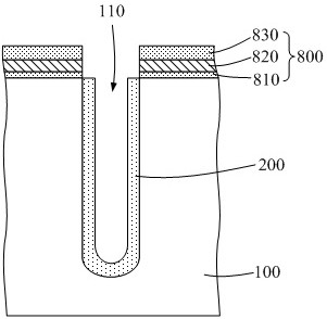
[0048] As mentioned in the background, when preparing the shielding electrode, because the electrode material is filled based on the trenches with a large aspect ratio, gaps are likely to be formed on the top of the filled electrode material layer. At this time, further When the electrode material layer is etched back, due to the existence of voids, the top surface of the formed shielding electrode will be further recessed, which cannot guarantee the stable performance of the finally prepared transistor device.

[0049] In order to improve the problem that the top surface of the shielding electrode is sunken due to the voids in the electrode material layer, a solution is to increase the slope of the sidewall of the trench to improve the filling performance of the trench, so as to alleviate the problem of filling the electrode material. It is easy to cause the problem of voids when layering. However, as the inclination of the sidewall of the trench increases, the size of the op...


PUM


Abstract

The invention provides a shielded gate field effect transistor, a forming method thereof, and a semiconductor device. A sacrificial layer is used to form a first dielectric layer in the lower trench of the trench to form a trench with a wide top and a narrow bottom, so that when the electrode material layer is filled, the gaps generated can be controlled to be located in the lower trench, avoiding the gap The existence of the electrode material layer affects the etching process of the electrode material layer, ensuring the performance of the formed transistor device. In addition, the formation method provided by the present invention can allow gaps in the electrode material layer, so that the sidewalls of the trenches can be vertical or nearly vertical sidewalls, which is beneficial to reduce the size of transistor devices.

Description

technical field [0001] The invention relates to the technical field of image sensors, in particular to a shielded gate field effect transistor, a forming method thereof, and a semiconductor device. Background technique [0002] A shielded gate field effect transistor (Shielded Gate Trench, SGT) is more conducive to the flexible application of semiconductor integrated circuits because of its low gate-to-drain capacitance Cgd, very low on-resistance, and high withstand voltage performance. Specifically, in the shielded gate field effect transistor, by setting the shielding electrode below the gate electrode, the gate-to-drain capacitance can be greatly reduced, and the drift region of the shielded gate field effect transistor also has a relatively high impurity carrier Concentration, can provide additional benefits to the breakdown voltage of the device, which can reduce the on-resistance accordingly. [0003] Wherein, the forming method of the shielded gate field effect tran...

Claims


Application Information

Patent Timeline
Patent Type & Authority Patents(China)
IPC IPC(8): H01L29/78H01L29/423H01L29/06H01L21/336
CPCH01L29/0603H01L29/0684H01L29/4236H01L29/66477H01L29/78
Inventor 李艳旭宋金星
Owner SEMICON MFG ELECTRONICS (SHAOXING) CORP
Why Eureka
Try Eureka