Capacitor structure, semiconductor device and capacitor structure preparation method

A capacitor structure and capacitor technology, which is applied in the field of semiconductor devices and capacitor structure preparation, capacitor structure, can solve the problems of supporting layer structure damage, affecting the stability of capacitor structure, high etch rate, etc.

Pending Publication Date: 2020-10-27
FUJIAN JINHUA INTEGRATED CIRCUIT CO LTD
View PDF0 Cites 8 Cited by
  • Summary
  • Abstract
  • Description
  • Claims
  • Application Information

AI Technical Summary

Problems solved by technology

[0003] In the prior art, carbon-containing materials are usually used as the support layer of the lower electrode, but the carbon-containing support layer will react during the subsequent deposition of the high-order dielectric layer, causing carbon pollution and resulting in a higher leakage rate of the capacitor
When a carbon-free material is used as the support layer of the lower electrode, the etching solution has a relatively high etching rate for the carbon-free support layer, so that in the process of patterning the top support structure of the lower electrode, The structure of the support layer will be damaged, affecting the structural stability of the capacitor

Method used


Image

  • Capacitor structure, semiconductor device and capacitor structure preparation method
  • Capacitor structure, semiconductor device and capacitor structure preparation method
  • Capacitor structure, semiconductor device and capacitor structure preparation method

Examples


Embodiment 1

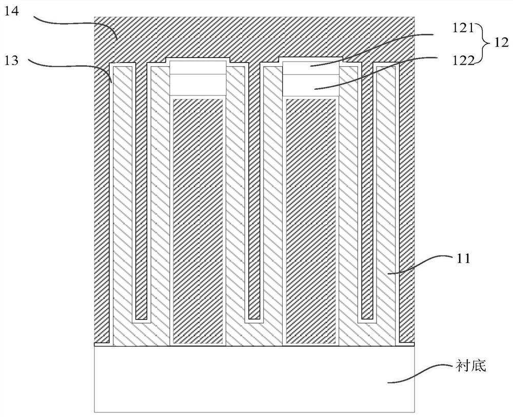
[0043] see figure 1 as shown, figure 1 A schematic cross-sectional structure diagram of a capacitance structure provided by an embodiment of the present application is shown, which includes:

[0044] The lower electrode 11, the lower electrode 11 has a columnar structure;

[0045] The support structure 12, the support structure 12 is located on the outer side wall of the lower electrode 11, wherein the support structure 12 includes a top support structure supporting the upper region of the lower electrode 11, the top support structure at least includes a first support layer 121 and materials with the first support layer 121 Different from the second supporting layer 122, the lower surface of the first supporting layer 121 is in contact with the upper surface of the second supporting layer 122, and the contact interface between the first supporting layer 121 and the second supporting layer 122 is lower than the top of the lower electrode 11, The upper surface of the first sup...

Embodiment 2

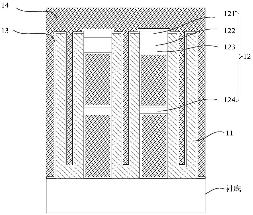
[0057] see figure 2 as shown, figure 2 It shows a schematic cross-sectional structure diagram of another capacitor structure provided by the embodiment of the present application. Compared with the capacitor structure provided by Embodiment 1 of the present application, the top support structure further includes a third support layer with a material different from that of the second support layer 122 123 , the upper surface of the third supporting layer 123 is in contact with the upper surface of the second supporting layer 122 . In addition, the supporting structure may further include an intermediate supporting structure supporting the middle region of the lower electrode 11 , wherein the intermediate supporting structure includes at least the fourth supporting layer 124 .

[0058] For the sake of brevity, the similarities between the capacitor structure provided in the second embodiment and the capacitor structure provided in the first embodiment will not be repeated, an...

Embodiment 3

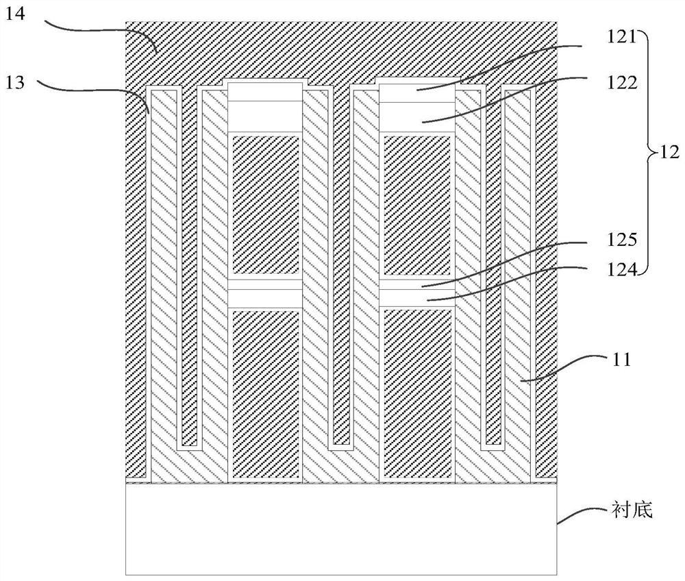
[0063] see image 3 as shown, image 3 A schematic cross-sectional structure diagram of another capacitor structure provided by the embodiment of the present application is shown. Compared with the capacitor structure provided by the first embodiment of the present application, the support structure 12 may also include an intermediate support structure supporting the middle region of the lower electrode 11 . For the sake of brevity, the similarities between the capacitor structure provided in the third embodiment and the capacitor structure provided in the first embodiment will not be repeated, and the differences between the third embodiment and the first embodiment will be mainly described below.

[0064] In the third embodiment of the present application, the intermediate support structure at least includes a fourth support layer 124 and a fifth support layer 125 of a material different from that of the fourth support layer 124, the upper surface of the fourth support layer...


PUM


Abstract

The invention discloses a capacitor structure, a semiconductor device and a capacitor structure preparation method. A supporting structure is arranged on the outer side wall of a lower electrode of acolumnar structure; the supporting structure comprises a top supporting structure for supporting the upper area of the lower electrode; the top supporting structure at least comprises a first supporting layer and a second supporting layer made of a material different from that of the first supporting layer. The lower surface of the first supporting layer is arranged to be in contact with the uppersurface of the second supporting layer, the contact interface of the first supporting layer and the second supporting layer is lower than the top of the lower electrode, and the upper surface of thefirst supporting layer is higher than the top of the lower electrode; a capacitor dielectric layer covering the lower electrode and the support structure and an upper electrode covering the capacitordielectric layer are formed, so the electric leakage rate can be reduced while the extending height of the lower electrode in the vertical direction is met, the supporting structure at the position needing to be reserved is prevented from being damaged in the patterning process of the top supporting structure of the lower electrode, and the stability of the lower electrode and the performance of the capacitor structure can be effectively improved.

Description

technical field [0001] The present application relates to the field of semiconductor technology, and in particular to a capacitance structure, a semiconductor device and a method for preparing the capacitance structure. Background technique [0002] Capacitors, as a semiconductor storage device, are constantly being miniaturized with the progress and requirements of the manufacturing process in the prior art. In order to ensure the storage capacity of the capacitor on the basis of miniaturization, it is usually necessary to extend the electrode in the vertical direction to the substrate, such as setting the lower electrode with a columnar structure, and setting the lower electrode extended in the vertical direction may easily cause the bottom electrode to tilt or bending. Therefore, it is necessary to provide a support structure outside the lower electrode to avoid deformation of the lower electrode. [0003] In the prior art, carbon-containing materials are usually used a...

Claims


Application Information

Patent Timeline
Patent Type & Authority Applications(China)
IPC IPC(8): H01L49/02
CPCH01L28/40H01L28/92
Inventor 蔡佩庭邢庸宇詹益旺刘安淇蔡东益
Owner FUJIAN JINHUA INTEGRATED CIRCUIT CO LTD
Why Eureka
Try Eureka