Processing method for back-to-back design of PCB

A technology of PCB board and processing method, applied in the processing field of PCB board back-to-back design, can solve the problems of inability to guarantee quality, long processing cycle, low production efficiency, etc. Effect

Pending Publication Date: 2020-10-27
BRAIN POWER (QING YUAN) CO LTD
View PDF1 Cites 4 Cited by
  • Summary
  • Abstract
  • Description
  • Claims
  • Application Information

AI Technical Summary

Problems solved by technology

[0002] With the rapid development of the electronics industry, the electronics industry has achieved diversification. In terms of product types, the PCB board industry is moving closer to high precision, high density and high reliability. Improve productivity and reduce pollution to adapt to the development of various downstream electronic equipment industries. Therefore, single-sided and double-sided boards are gradually developing into multi-layer boards. Multi-layer boards have high assembly density and small size; the connection between electronic components is shortened , the signal transmission speed is improved; convenient wiring and many other advantages, but the more layers, the higher the cost, and the longer the processing cycle
[0003] The Chinese patent discloses a PCB board processing method and PCB board (authorized announcement number CN104470211A). The patented technology shows that the coated surface coating layer does not need to go through a high-temperature pressing process without being damaged, and the solderability of the finished PCB board is not affected. Affected, but its production efficiency is low, delivery time is slow, and the quality is not guaranteed.

Method used


Image

  • Processing method for back-to-back design of PCB

Examples


Embodiment Construction

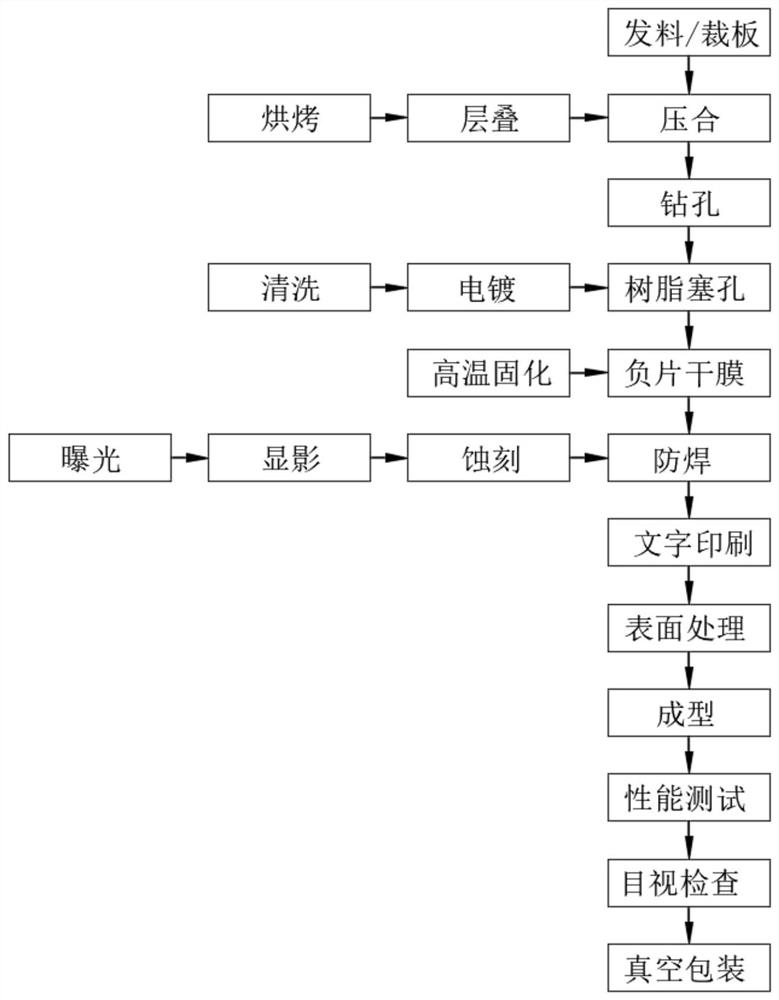
[0025] see figure 1 , in an embodiment of the present invention, a back-to-back design processing method for a PCB includes an upper core board and several layers of middle core boards located at the bottom of the upper core board, the bottom of the middle core board is provided with a lower core board, the The size of the upper core board, the middle core board and the lower core board are all the same.

[0026] In this embodiment, preferably, copper layers are electroplated on the front and back sides of the upper core board, the middle core board and the lower core board.

[0027] In this embodiment, preferably, a semi-cured prepreg material is provided between the upper core board and the middle core board, between each middle core board, and between the middle core board and the lower core board.

[0028] In this embodiment, preferably, its implementation method includes the following steps:

[0029] S1: Select the appropriate material according to the needs, and cut an...


PUM


Abstract

The invention relates to the technical field of PCB processing. The invention discloses a processing method for back-to-back design of a PCB. The method comprises an upper core plate and a plurality of middle core plates positioned at the bottom end of the upper core plate, a lower-layer core plate is arranged at the bottom end of the middle-layer core plate; the sizes of the upper core plate, themiddle core plate and the lower core plate are the same; copper layers are electroplated on the front surfaces and the back surfaces of the upper-layer core plate, the middle-layer core plate and thelower-layer core plate, and semi-cured prepreg materials are arranged between the upper-layer core plate and the middle-layer core plate, between the middle-layer core plates and between the middle-layer core plates and the lower-layer core plate. According to the invention, before pressing combination, one core plate is normally stacked and the other core plate is combined back to back after being rotated by 180 degrees and then is pressed, so that the use amount of films can be greatly reduced, the utilization rate of the screen plate can be reduced, the production cost is reduced, the processing time is saved, the production efficiency is improved, the delivery rate is ensured, the quality is ensured, and the market requirements are met.

Description

technical field [0001] The invention relates to the technical field of PCB board processing, in particular to a processing method for back-to-back design of PCB boards Background technique [0002] With the rapid development of the electronics industry, the electronics industry has achieved diversification. In terms of product types, the PCB board industry is moving closer to high precision, high density and high reliability. Improve productivity and reduce pollution to adapt to the development of various downstream electronic equipment industries. Therefore, single-sided and double-sided boards are gradually developing into multi-layer boards. Multi-layer boards have high assembly density and small size; the connection between electronic components is shortened , the signal transmission speed is improved; convenient wiring and many other advantages, but the more layers, the higher the cost, and the longer the processing cycle. [0003] The Chinese patent discloses a PCB bo...

Claims


Application Information

Patent Timeline
Patent Type & Authority Applications(China)
IPC IPC(8): H05K3/46H05K3/02
CPCH05K3/022H05K3/4644
Inventor 郑朝屹黄蝉廖强
Owner BRAIN POWER (QING YUAN) CO LTD
Why Eureka
Try Eureka