Semiconductor structure and forming method thereof

A technology of semiconductor and gate structure, applied in the field of semiconductor structure and its formation, can solve the problem that the surface of the wafer cannot provide enough area for interconnection lines, etc., so as to reduce the probability of bridging and optimize the electrical performance.

Pending Publication Date: 2020-10-30
SEMICON MFG INT (SHANGHAI) CORP +1
View PDF0 Cites 0 Cited by
  • Summary
  • Abstract
  • Description
  • Claims
  • Application Information

AI Technical Summary

Problems solved by technology

In order to improve integration and reduce costs, the critical dimensions of components are continuously reduced, and the circuit density inside in...

Method used


Image

  • Semiconductor structure and forming method thereof
  • Semiconductor structure and forming method thereof
  • Semiconductor structure and forming method thereof

Examples


Embodiment Construction

[0013] It can be seen from the background art that the devices formed so far still have the problem of poor performance. The reasons for the poor performance of the device are analyzed in conjunction with a method of forming a semiconductor structure.

[0014] refer to Figure 1 to Figure 4 A structural schematic diagram corresponding to each step in a method for forming a semiconductor structure is shown.

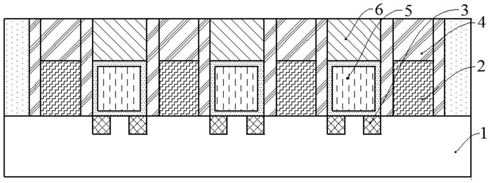
[0015] Such as figure 1 As shown, a substrate is provided, and the substrate includes a substrate 1, a gate structure 2 located on the substrate 1, source and drain doped regions 3 located in the substrate 1 on both sides of the gate structure 2, An insulating cap layer 4 on the gate structure 2, a source-drain connection layer 5 on the substrate 1 between the insulating cap layers 4, and a source-drain dielectric layer on the source-drain connection layer 5 Layer 6.

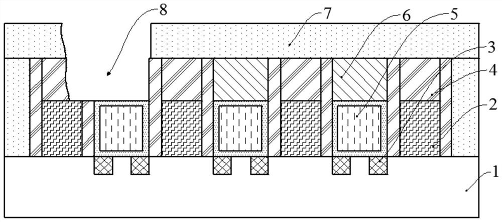
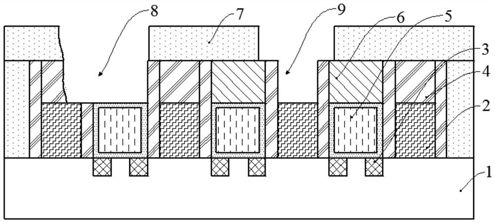
[0016] Such as figure 2 As shown, an interlayer dielectric layer 7 is formed on the insulating capp...


PUM

PropertyMeasurementUnit
Thicknessaaaaaaaaaa

Abstract

The invention discloses a semiconductor structure and a forming method. The forming method comprises the steps of providing a base, wherein the base comprises a substrate, a gate structure located onthe substrate, an insulating cap layer located on the gate structure, and a source-drain connecting layer located on the substrate between the gate structures, wherein the top surface of the source-drain connecting layer is lower than the top surface of the insulating cap layer; forming an etching stop layer on the insulating cap layer; forming a source-drain dielectric layer on the source-drain connecting layer; removing the source-drain dielectric layer on the source-drain connecting layer by adopting a first etching process to form a first opening, wherein in the first etching process, theetched rate of the insulating cap layer is less than the etched rate of the source-drain dielectric layer, and the etched rate of the etching stop layer is less than the etched rate of the insulatingcap layer; and forming a source-drain contact hole plug in the first opening. In the process of forming the first opening, the etching stop layer is not easy to etch and remove, the probability of bridging between the source-drain contact hole plug and the gate structure is reduced, and the electrical performance of the semiconductor structure is optimized.

Description

technical field [0001] Embodiments of the present invention relate to the field of semiconductor manufacturing, and in particular, to a semiconductor structure and a method for forming the same. Background technique [0002] With the continuous development of integrated circuit manufacturing technology, people's requirements for the integration and performance of integrated circuits are becoming higher and higher. In order to improve integration and reduce costs, the critical dimensions of components are getting smaller and the circuit density inside integrated circuits is increasing. This development makes the surface of the wafer unable to provide enough area to make the required interconnection lines. [0003] In order to meet the requirements of the interconnection line after the critical dimension is reduced, at present, the conduction between different metal layers or between the metal layer and the substrate is realized through the interconnection structure. The inte...

Claims


Application Information

Patent Timeline
IPC IPC(8): H01L21/786H01L21/8234
CPCH01L21/76897H01L21/823431H01L21/823475
Inventor 张海洋纪世良
Owner SEMICON MFG INT (SHANGHAI) CORP
Why Eureka
Try Eureka