
Integrated circuit and method of forming semiconductor structure

A technology for integrated circuits and semiconductors, which is applied in semiconductor devices, semiconductor/solid-state device manufacturing, circuits, etc., and can solve problems such as inapplicability of thick gate dielectric layers and limiting the thickness of gate dielectric layers.

Pending Publication Date: 2020-10-30
TAIWAN SEMICON MFG CO LTD
View PDF0 Cites 0 Cited by
  • Summary
  • Abstract
  • Description
  • Claims
  • Application Information

AI Technical Summary

Problems solved by technology

The vertical space between adjacent wire channels or sheet channels limits the thickness of the gate dielectric layer
Therefore, GAA NW devices and GAA NS devices may not be suitable for certain applications that require thick gate dielectric layers, such as input / output (I / O) functions

Method used


Image

  • Integrated circuit and method of forming semiconductor structure
  • Integrated circuit and method of forming semiconductor structure
  • Integrated circuit and method of forming semiconductor structure

Examples


Embodiment Construction

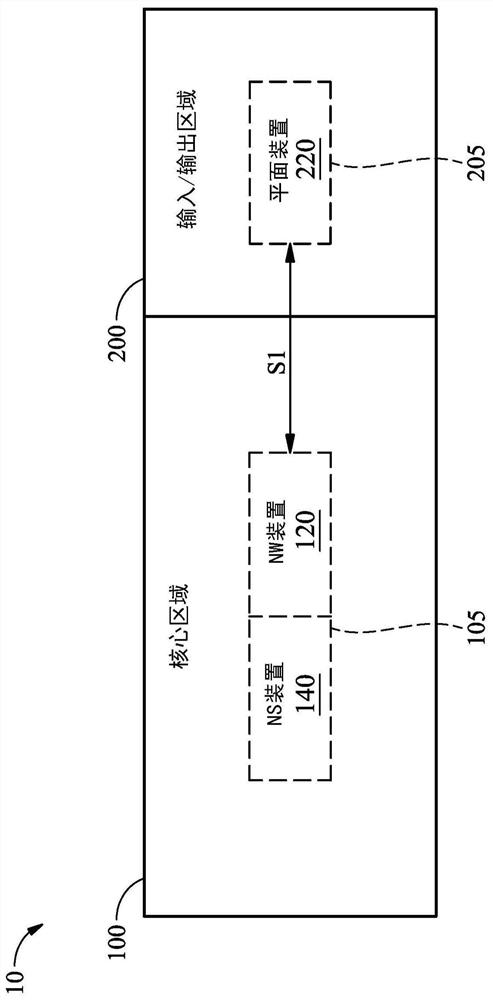
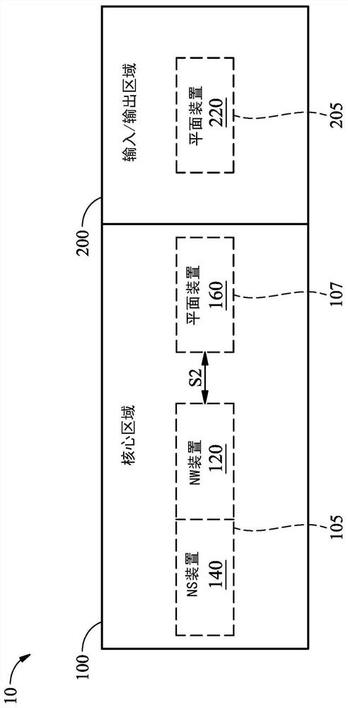
[0065] The following disclosure provides many different embodiments, or examples, for implementing different features of the presented subject matter. Specific examples of components and arrangements are described below to simplify the present disclosure. Of course, these are examples only and are not intended to be limiting. For example, in the description below, forming a first feature over or on a second feature may include embodiments where the first and second features are formed in direct contact, and may also include embodiments in which the first and second features are formed Embodiments where additional features are formed such that the first and second features may not be in direct contact. In addition, the present disclosure may repeat element symbols and / or letters in various examples. This repetition is for brevity and clarity and does not in itself indicate a relationship between the various embodiments and / or configurations discussed.

[0066] In addition, f...


PUM

PropertyMeasurementUnit
thicknessaaaaaaaaaa
thicknessaaaaaaaaaa
thicknessaaaaaaaaaa

Abstract

The embodiment of the invention provides an integrated circuit and a method for forming a semiconductor structure. The gate-all-around (GAA) nanowire transistor is provided with a plurality of nanowire channels which are vertically stacked, a first grid dielectric layer wrapping the nanowire channels and a first grid electrode wrapping the first grid dielectric layer. The GAA nanowire transistorshas a plurality of vertically stacked nanosheet channels, a second gate dielectric layer wrapping the nanosheet channels, and a second gate electrode wrapping the second gate dielectric layer. The planar device has a planar channel, a third gate dielectric layer on the planar channel, and a third gate electrode on the third gate dielectric layer. The first and second gate dielectric layers have the same thickness. The third gate dielectric layer is thicker than the first and second gate dielectric layers. The widths of the nanowire channels and the nanosheet channels are smaller than the widthof the planar channel.

Description

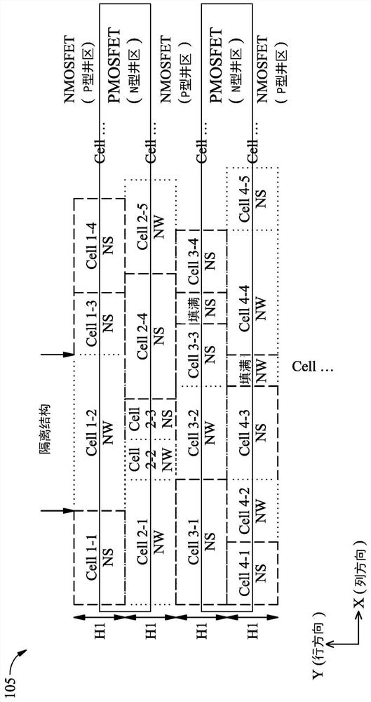
technical field [0001] The present disclosure relates to a semiconductor device, and more particularly to a semiconductor device having a wrap-around gate device and a planar device. Background technique [0002] Vertically stacked gate-all-around (GAA) horizontal nanowire (NW) and nanosheet (nanosheet, NS) devices are promising next-generation integrated circuits (ICs) because of their Good gate controllability, low leakage and good scalability. The GAA NW device and the GAA NS device have multiple vertically stacked wire channels and sheet channels, respectively, in their channel region, which are wrapped by gate dielectric layers and gate electrodes. The vertical space between adjacent wire channels or sheet channels limits the thickness of the gate dielectric layer. Therefore, GAA NW devices and GAA NS devices may not be suitable for certain applications requiring thick gate dielectric layers, such as input / output (I / O) functions. Improvements are needed in this area....

Claims


Application Information

Patent Timeline
Patent Type & Authority Applications(China)
IPC IPC(8): H01L27/06H01L27/092H01L29/06H01L21/822H01L21/8238
CPCH01L27/06H01L27/0928H01L29/0665H01L29/0669H01L21/822H01L21/823857H01L21/823807H01L29/78696H01L29/42392H01L27/088H01L21/823412H01L27/0922H01L29/0673H01L29/775B82Y10/00H01L27/092
Inventor 廖忠志
Owner TAIWAN SEMICON MFG CO LTD
Learn More