Superconducting tunnel junction, superconducting electronic component and preparation method thereof

A tunnel junction and superconducting technology, which is applied in the manufacture/processing of superconductor components and superconductor devices, can solve problems such as inability to meet the requirements for the use of ultra-high frequency oscillators, low resonance frequency, and inability to meet application requirements.

Pending Publication Date: 2020-10-30
SIEN QINGDAO INTEGRATED CIRCUITS CO LTD
View PDF0 Cites 0 Cited by
  • Summary
  • Abstract
  • Description
  • Claims
  • Application Information

AI Technical Summary

Problems solved by technology

[0003] The superconductors of the superconducting tunnel junction in the prior art are generally made of the same material. Such a superconducting tunne

Method used


Image

  • Superconducting tunnel junction, superconducting electronic component and preparation method thereof
  • Superconducting tunnel junction, superconducting electronic component and preparation method thereof
  • Superconducting tunnel junction, superconducting electronic component and preparation method thereof

Examples


Embodiment 1

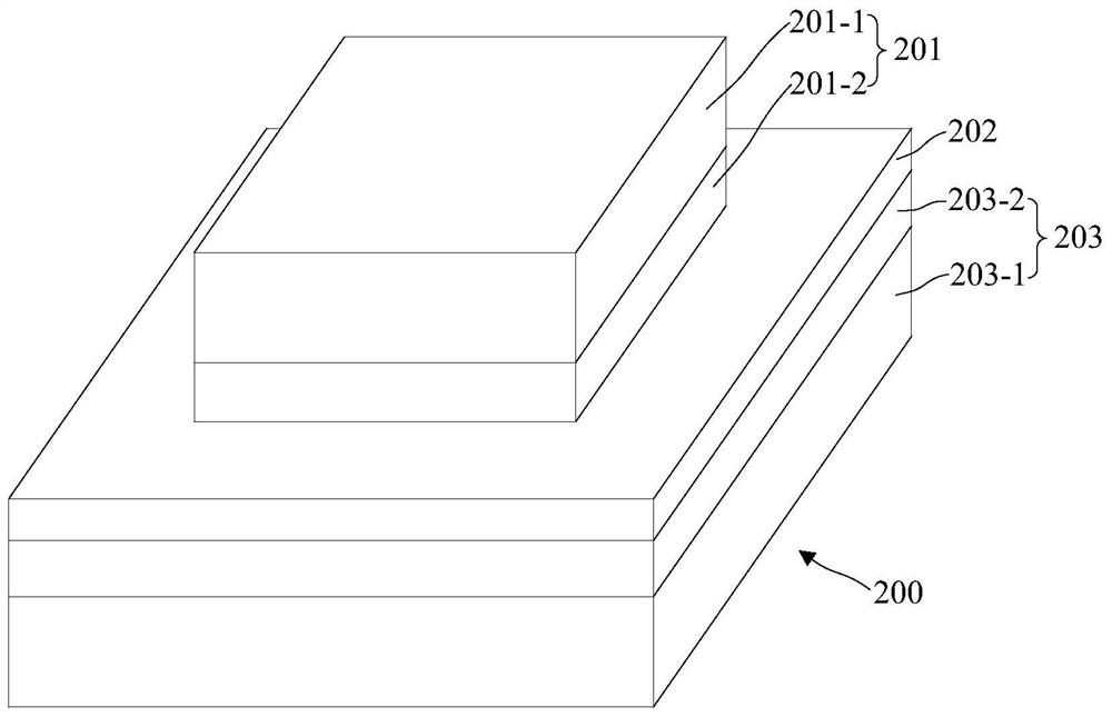
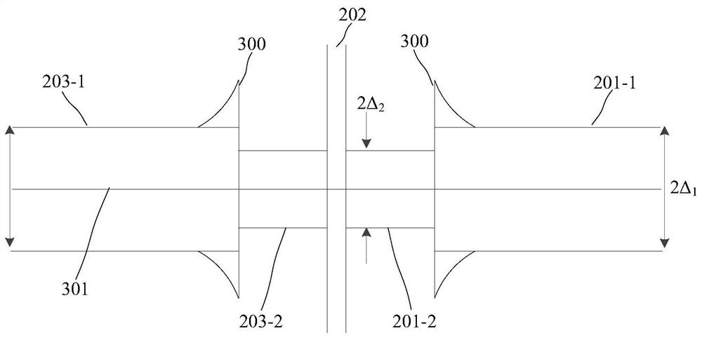
[0079] This embodiment provides a superconducting tunnel junction, such as figure 2 As shown, the superconducting tunnel junction 200 includes a lower electrode 203 , a dielectric layer 202 formed on the lower electrode 203 , and an upper electrode 201 formed on the dielectric layer 202 . Both the upper electrode 201 and the lower electrode 203 include a multilayer structure, the multilayer structure includes layers of different superconducting materials, the superconducting tunnel junction forms a heterogeneous superconducting tunnel junction, and from the dielectric layer to the direction of the upper electrode and the lower electrode, i.e. figure 2 In the direction of the arrow R shown, the energy band widths of the different superconducting materials of the multilayer structure gradually increase.

[0080] In a preferred embodiment of this embodiment, as figure 2 As shown, both the upper electrode 201 and the lower electrode 203 include a two-layer structure. Specifi...

Embodiment 2

[0090] This embodiment provides a superconducting electronic element, such as Figure 5 As shown, the superconducting electronic element 400 includes a substrate 401 and at least one superconducting tunnel junction 402 formed on the substrate 401 (for convenience of illustration, Figure 5 Only one of the superconducting tunnel junctions is shown). At least one superconducting tunnel junction is electrically connected in series and / or in parallel.

[0091] The substrate 401 may be a commonly used substrate such as single crystal silicon, sapphire, silicon carbide, silicon dioxide on single crystal silicon, and the like. The thickness of the substrate 401 can be between 0.2mm-0.7mm, and of course the thickness of the substrate 401 can be selected according to actual needs.

[0092] The superconducting tunnel junction 402 includes a lower electrode 402-1, a dielectric layer 402-2 formed on the lower electrode, and an upper electrode 402-3 formed on the dielectric layer 402-2. ...

Embodiment 3

[0097] This embodiment provides a method for preparing a superconducting electronic element, such as Figure 8 As shown, the method includes the following steps:

[0098] providing a substrate on which a patterned masking layer is formed;

[0099] forming a lower electrode on the substrate through the patterned mask layer;

[0100] forming a dielectric layer on the lower electrode;

[0101] forming an upper electrode on the dielectric layer;

[0102] Wherein, the upper electrode and the lower electrode include a superconducting material, the upper electrode, the dielectric layer, and the lower electrode form a superconducting tunnel junction, and both the upper electrode and the lower electrode include a multi- a layer structure, the multilayer structure includes layers of different superconducting materials, and in the direction from the dielectric layer to the upper electrode and the lower electrode, the different superconducting materials of the multilayer structure The...


PUM

PropertyMeasurementUnit
Lengthaaaaaaaaaa
Widthaaaaaaaaaa
Thicknessaaaaaaaaaa

Abstract

The invention provides a superconducting tunnel junction, a superconducting electronic component and a preparation method thereof. The superconducting tunnel junction comprises a lower electrode, a dielectric layer formed on the lower electrode, and an upper electrode formed above the dielectric layer, wherein the lower electrode and the upper electrode respectively comprise a multi-layer structure, and the multi-layer structure comprises different superconducting material layers. The superconducting tunnel junction forms a heterogeneous superconducting tunnel junction, and superconducting energy bands of multiple layers of different superconducting materials are gradually increased in the direction from the dielectric layer to the upper electrode and the lower electrode. In a Josephson tunnel junction formed by an upper electrode and a lower electrode which are both of a two-layer structure and an electronic component comprising the Josephson tunnel junction, the interfacial energy band difference of heterogeneous superconducting materials and the Andreev reflection interact, and a second type superconducting material Josephson tunnel junction between two layers of first type superconducting materials forms a resonant cavity. The resonant frequency of the resonant cavity can reach 500GHz-900GHz, and a gap band between a submicron wave and an infrared spectrum is filled, so that the resonant cavity can be applied to a broadband ultrahigh frequency oscillator.

Description

technical field [0001] The invention relates to the technical field of superconducting electronic components, in particular to a superconducting tunnel junction, a superconducting electronic component and a preparation method thereof. Background technique [0002] When two metals are separated by a thin layer of insulator, current can flow between the metals, and this "metal-insulator-metal" stack is usually called a tunnel junction. An insulating layer is embedded between two superconductors to form a Josephson tunnel junction. The two superconductors form a weak coupling through the intermediate insulating layer, and the superconducting electrons can pass through the semiconductor or insulator film from one side to the other side through the tunnel effect. [0003] The superconductors of the superconducting tunnel junction in the prior art are generally made of the same material, and such a superconducting tunnel junction has a low resonant frequency, which cannot meet so...

Claims


Application Information

Patent Timeline
IPC IPC(8): H01L39/02H01L39/24
CPCH10N60/80H10N60/01
Inventor 王津洲
Owner SIEN QINGDAO INTEGRATED CIRCUITS CO LTD
Why Eureka
Try Eureka