Fingerprint identification device and electronic equipment

A fingerprint recognition, fingerprint technology

Pending Publication Date: 2020-11-03
SHENZHEN GOODIX TECH CO LTD
View PDF0 Cites 3 Cited by
  • Summary
  • Abstract
  • Description
  • Claims
  • Application Information

AI Technical Summary

Problems solved by technology

With this technical solution, the overall light input of the fingerprint recognition device is small, the exposure time is long, the overall imaging quality is poor, and the recognition performance for dry fingers is not good.
At the same time, the thickness of the optical path in the fingerprint identification device is thick, which increases the processing difficulty and cost of the optical path, and is not conducive to the development of thinner and lighter fingerprint identification devices.

Method used


Image

  • Fingerprint identification device and electronic equipment
  • Fingerprint identification device and electronic equipment
  • Fingerprint identification device and electronic equipment

Examples


Embodiment Construction

[0083] The technical solutions in the embodiments of the present application will be described below with reference to the accompanying drawings.

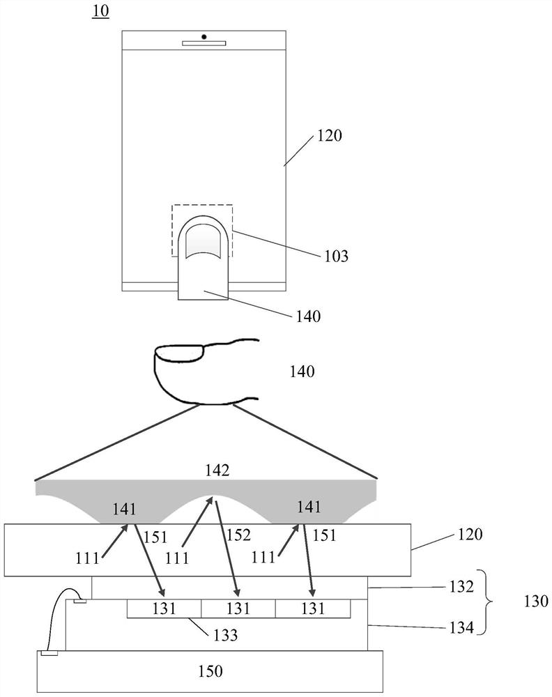
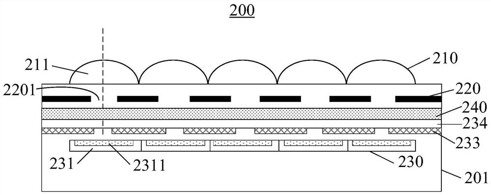
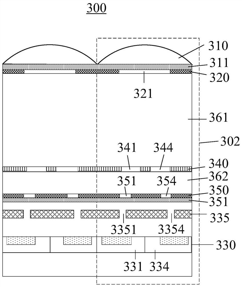
[0084] It should be understood that the embodiments of the present application can be applied to optical fingerprint systems, including but not limited to optical fingerprint recognition systems and products based on optical fingerprint imaging. The embodiments of the present application only take the optical fingerprint system as an example for description, but should not be implemented in this application. The examples constitute any limitation, and the embodiments of the present application are also applicable to other systems using optical imaging technology, and the like.

[0085] As a common application scenario, the optical fingerprint system provided in the embodiments of the present application can be applied to smart phones, tablet computers, and other mobile terminals or other electronic devices with display screens; more s...


PUM


Abstract

The invention discloses a fingerprint identification device and electronic equipment, which can improve the performance of the fingerprint identification device and reduce the cost. The fingerprint identification device comprises: a fingerprint identification module, which comprises a micro lens; at least two diaphragm layers, wherein each of the at least two diaphragm layers is provided with a light through hole to form a plurality of light guide channels in different directions, and in the at least two diaphragm layers, the non-light-through hole area of at least one first diaphragm layer isused for absorbing visible light, and the non-light-through hole area of at least one second diaphragm layer is used for absorbing visible light; the non-light-transmitting hole area of at least onesecond diaphragm layer is used for transmitting non-pixel sensitive light and absorbing the pixel sensitive light; a plurality of pixel units is arranged below the at least two diaphragm layers and ispositioned at the bottoms of the plurality of light guide channels; wherein after fingerprint optical signals returned after being reflected or scattered by a finger above the display screen are converged through the micro lens, a plurality of target fingerprint optical signals in different directions are respectively transmitted to the plurality of pixel units through the plurality of light guide channels, and the plurality of target fingerprint optical signals are used for detecting fingerprint information of the finger.

Description

technical field [0001] The present application relates to the field of optical fingerprint technology, and more particularly, to a fingerprint identification device and an electronic device. Background technique [0002] With the rapid development of the mobile phone industry, the application of under-screen optical fingerprint technology solutions is becoming more and more popular, and terminal manufacturers have a strong demand for solutions with thinner thickness, lower performance and lower cost. [0003] In some related technologies, the microlens array in the fingerprint identification device is located directly above the pixel array, and one microlens corresponds to one pixel unit, that is, each microlens in the microlens array focuses the received light to the same microlens In the corresponding pixel unit, a plurality of pixel units are arranged in an array. With this technical solution, the overall light input amount of the fingerprint identification device is sma...

Claims


Application Information

Patent Timeline
IPC IPC(8): G06K9/00
CPCG06V40/1324
Inventor 蒋鹏
Owner SHENZHEN GOODIX TECH CO LTD
Why Eureka
Try Eureka