
Micro-semiconductor stacked structure and electronic device thereof

A stacked structure and semiconductor technology, applied in the direction of semiconductor devices, circuits, electrical components, etc., can solve problems such as cost and technical bottlenecks

Pending Publication Date: 2020-11-03
LG DISPLAY CO LTD
View PDF0 Cites 5 Cited by
  • Summary
  • Abstract
  • Description
  • Claims
  • Application Information

AI Technical Summary

Problems solved by technology

With the pursuit of high resolution (more pixels with a limited area), the length and width of pixels have been reduced to the micron level. Even so, they still suffer from cost and technical bottlenecks, and the industry urgently needs to propose a new solution.

Method used


Image

  • Micro-semiconductor stacked structure and electronic device thereof
  • Micro-semiconductor stacked structure and electronic device thereof
  • Micro-semiconductor stacked structure and electronic device thereof

Examples


no. 1 example

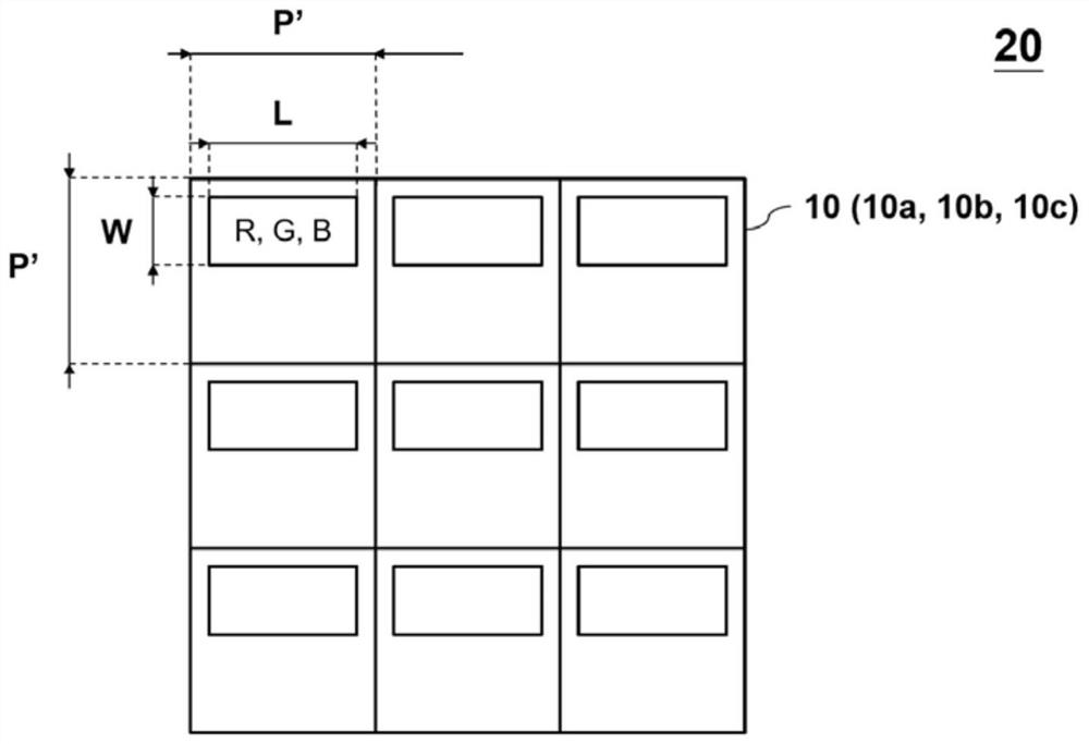
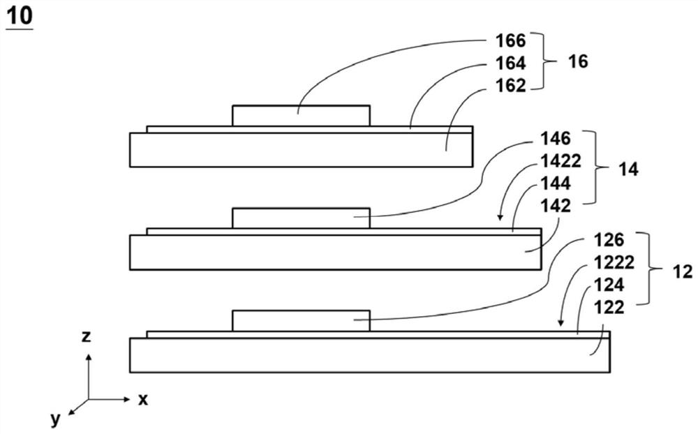
[0055] The invention discloses a micro-semiconductor stacked structure comprising three stacked structures, wherein two stacked structures are superimposed on the lowest stacked structure; wherein the two stacked structures are stacked along the vertical direction of the bottom stacked structure; each stacked structure includes a base material , a conductive layer arranged on the substrate, and a micro light-emitting diode chip arranged on the substrate and electrically connected to the conductive layer. Each stacked structure defines a pixel, and the micro light-emitting diode chips in each stacked structure are arranged in the pixel; the target areas between two stacked structures are aligned with each other along the aforementioned vertical direction; in at least one stacked structure of the three stacked structures, the conductive Layers are active circuits. For details, please also refer to figure 2 and Figure 3A , 3B , discloses the micro-semiconductor stack structu...

no. 2 example

[0070] see also figure 2 and Figure 4A , Figure 4B , discloses a micro-semiconductor stack structure 10a according to a second embodiment of the present invention, and an electronic device 20a composed of a plurality of micro-semiconductor stack structures 10a array. In this embodiment, the micro-semiconductor stack structure 10a and the electronic device 20a are similar to the micro-semiconductor stack structure 10 and the color display unit of the first embodiment; only the differences from the first embodiment are disclosed below: as Figure 4A , the micro-semiconductor stack structure 10a has a first stack structure 12a, a second stack structure 14a, and a third stack structure 16a; the first base material 122a of the first stack structure 12a, the second base material 142a of the second stack structure 14a, The third substrate 162a of the third laminated structure 16a is a flexible transparent substrate, such as Polyimide, PEN, PET or their equivalents, and the thick...

no. 3 example

[0075] see also figure 2 and Figure 5 , discloses the micro-semiconductor stack structure 10b and its electronic device 20b according to the third embodiment of the present invention. In this embodiment, the micro-semiconductor stack structure 10b is a mixture of the materials, processes and structures of the micro-semiconductor stack structure 10 of the first embodiment and the micro-semiconductor stack structure 10a of the third embodiment; The difference between the three embodiments: as Figure 5 The micro-semiconductor stack structure 10b has a first stack structure 12b, a second stack structure 14b and a third stack structure 16b; the first stack structure 12b is selected from the first substrate 122 in the micro-semiconductor stack structure 10 of the first embodiment, and Both the second stacked structure 14b and the third stacked structure 16b are selected from the second substrate 142a and the third substrate 162a in the micro-semiconductor stacked structure 10a ...


PUM

PropertyMeasurementUnit
sizeaaaaaaaaaa

Abstract

The invention relates to a micro-semiconductor stacked structure and an electronic device thereof. The invention provides a micro-semiconductor stacked structure which comprises at least two stacked structure array units, and one stacked structure array unit is stacked on the other stacked structure array unit, wherein one stacked structure array unit is stacked along the vertical direction of theother stacked structure array unit; each laminated structure array unit comprises a base material, a conductive pattern layer arranged on the base material, and a plurality of micro semiconductor devices arranged on the base material and electrically connected with the conductive pattern layer.

Description

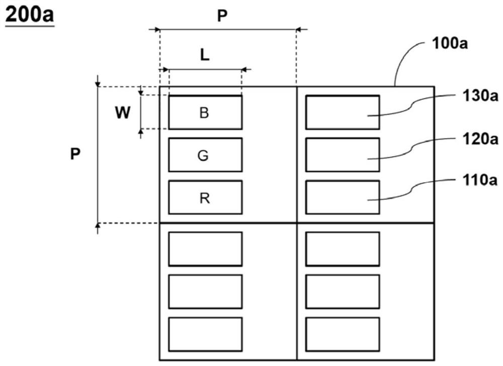
technical field [0001] The invention relates to an electronic device, in particular to an electronic device composed of a micro-semiconductor stack structure array. Background technique [0002] Generally, semiconductor arrays are arranged along a plane. Under the demand for components with smaller areas, the continuous improvement of process capabilities to achieve smaller line widths has always been the goal of semiconductor-related manufacturers. Due to the balance between cost and equipment investment in the industry , the advancement of the minimum line width has slowed down. [0003] Taking micro-light-emitting diode display technology as an example, such as figure 1 The red, green and blue light emitting diodes are respectively three sub-pixels 110a, 120a and 130a, which are adjacently arranged in a plane to form a pixel 100a, and a plurality of pixels 100a are arrayed to form a display 200a. Taking three micro-LEDs of the same size as an example, the micro-LEDs hav...

Claims


Application Information

Patent Timeline
Patent Type & Authority Applications(China)
IPC IPC(8): H01L25/075H01L25/065H01L33/62H01L31/02
CPCH01L25/0756H01L25/0753H01L33/62H01L25/0652H01L31/02005H01L27/15H01L33/24H01L27/156
Inventor 陈显德
Owner LG DISPLAY CO LTD
Learn More