IGZO (Indium Gallium Zinc Oxide) backboard structure applied to OLED (Organic Light Emitting Diode) panel and manufacturing method

A manufacturing method and backplane technology, applied in the field of OLED display, can solve the problems of large leakage current, low resolution, low electron mobility, etc., and achieve the effects of reducing plane space, reducing pixel area, and improving resolution

Pending Publication Date: 2022-05-20
FUJIAN HUAJIACAI CO LTD
View PDF0 Cites 0 Cited by
  • Summary
  • Abstract
  • Description
  • Claims
  • Application Information

AI Technical Summary

Problems solved by technology

Although the electron mobility of LTPS is large, the leakage current is also large, so the capacitor needs to be frequently charged to keep the current driving the OLED element stable during display, and the driving power consumption is high, so it is not suitable for low-frequency refresh
In addition, the manufacturing cost of the LTPS backplane is also high, and the uniformity performance is not good, which is not suitable for the manufacture of large-size panels
[0003] The IGZO backplane has lower electron mobility than LTPS. To achieve the same on-state current as LTPS, larger-sized components are required, and the single sub-pixel driving circuit is larger, so the resolution is also lower.

Method used


Image

  • IGZO (Indium Gallium Zinc Oxide) backboard structure applied to OLED (Organic Light Emitting Diode) panel and manufacturing method
  • IGZO (Indium Gallium Zinc Oxide) backboard structure applied to OLED (Organic Light Emitting Diode) panel and manufacturing method

Examples


Embodiment Construction

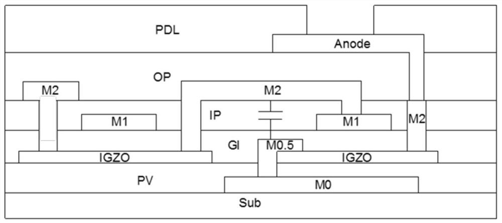
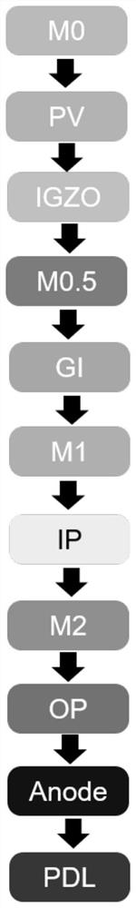
[0040] Please refer to figure 1 , the present invention is an IGZO backplane structure applied to an OLED panel, which includes a substrate Sub;

[0041] A metal layer M0 is provided on the substrate Sub, and the metal layer M0 is used to receive an OVDD signal;

[0042] An insulating layer PV is also provided on the substrate Sub, and the insulating layer PV covers the metal layer M0;

[0043] A semiconductor layer IGZO is disposed on the insulating layer PV;

[0044] A metal layer M0.5 is provided on the IGZO semiconductor layer, and the metal layer M0.5 is connected to the metal layer M0;

[0045] An insulating layer GI is also provided on the insulating layer PV, and the insulating layer GI covers the metal layer M0.5 and the semiconductor layer IGZO;

[0046] A metal layer M1 is disposed on the insulating layer GI, and the metal layer M1 is used for receiving SCAN scanning signals;

[0047] An insulating layer IP is further provided on the insulating layer GI, and the...


PUM


Abstract

The invention discloses an IGZO backboard structure applied to an OLED panel and a manufacturing method. A metal layer M0 is arranged on a substrate Sub; an insulating layer PV is also arranged on the substrate Sub, and the insulating layer PV covers the metal layer M0; a semiconductor layer IGZO is arranged on the insulating layer PV; a metal layer M0.5 is arranged on the IGZO semiconductor layer; an insulating layer GI is also arranged on the insulating layer PV and covers the metal layer M0.5 and the semiconductor layer IGZO; a metal layer M1 is arranged on the insulating layer GI; an insulating layer IP is also arranged on the insulating layer GI and covers the metal layer M1; a metal layer M2 is arranged on the insulating layer IP, and the metal layer M2 and the metal layer M0.5 form a storage capacitor; an organic flat layer OP is further arranged on the insulating layer IP, and the metal layer M2 is covered with the organic flat layer OP; an anode metal layer Anode is arranged on the organic flat layer OP; a pixel definition layer PDL is further arranged on the organic leveling layer OP, and an opening is formed in the position, at the anode metal layer Anode, of the pixel definition layer PDL. According to the invention, the defect of low resolution of the IGZO OLED panel can be improved.

Description

technical field [0001] The invention relates to the field of OLED display technology, in particular to an IGZO back plate structure and a manufacturing method applied to an OLED panel. Background technique [0002] At present, OLED panels on the market mainly use LTPS to drive the backplane. LTPS has the advantage of high electron mobility, which means that the smaller component size can reach the same on-state current as other semiconductor TFTs, and the pixel drive circuit can be made smaller. The resolution is also higher. Although the electron mobility of LTPS is large, the leakage current is also large, so the capacitor needs to be frequently charged to keep the current driving the OLED element stable during display, and the driving power consumption is high, so it is not suitable for low-frequency refresh. In addition, the manufacturing cost of the LTPS backplane is also high, and the poor uniformity performance is not suitable for the manufacture of large-size panels...

Claims


Application Information

Patent Timeline
Patent Type & Authority Applications(China)
IPC IPC(8): H01L27/12H01L27/32H01L21/84
CPCH01L27/124H01L27/1259H10K59/131H10K59/1201Y02E10/549
Inventor 杨远直罗敬凯贾浩
Owner FUJIAN HUAJIACAI CO LTD
Why Eureka
Try Eureka