Photovoltaic solder strip and photovoltaic module
A technology of photovoltaic ribbons and ribbons, which is applied in photovoltaic power generation, electrical components, semiconductor devices, etc., can solve the problem of color inconsistency between photovoltaic cells and backplanes, inability to apply component glare requirements, and affecting the aesthetics of photovoltaic modules, etc. problems, to achieve the effect of improving welding flexibility, improving uniformity and stability, and improving aesthetics
- Summary
- Abstract
- Description
- Claims
- Application Information
AI Technical Summary
Problems solved by technology
Method used
Image
Examples
no. 1 approach
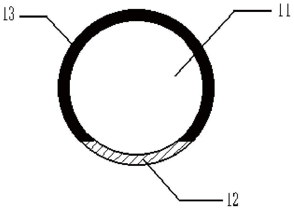
[0055] see Figure 2A-Figure 2C , which respectively show cross-sectional views of the first segment 101 , the second segment 103 and the third segment 104 of the photovoltaic ribbon according to the first embodiment of the present invention.
[0056] The solder ribbon comprises a base body 11 (conductive base material) wherein, in a first segment 101, a layer of solder is applied on the bottom surface of the first segment in order to enable the first segment to be bonded to the front side of the photovoltaic cell sheet 12; In addition, a black coating (for example, black paint) 13 is coated on other surfaces of the first segment body except the bottom surface, so that the first segment body 101 of the photovoltaic ribbon is bonded to the front side of the battery sheet The appearance is black and does not produce reflections.
[0057] Such as Figure 1B As shown, since the third segment body 104 needs to be bonded to the back of the adjacent battery sheet, therefore, as F...
Embodiment approach 1
[0063] In the first alternative embodiment of the present invention, in order to simplify the process, preferably, see Figure 4A-Figure 4C , which respectively show cross-sectional views of the first segment 101 , the second segment 103 and the third segment 104 according to the first alternative embodiment of the present invention.
[0064] Such as Figure 4A-Figure 4C As shown, the entire surfaces of the first segment body 101 , the second segment body 103 and the third segment body 104 are coated with the solder layer 12 . Wherein, in the first segment body 101, on other surface parts except the bottom surface, a black coating layer 13 is further coated above the solder layer 12; in the second segment body 103, the solder layer 12 on the entire surface is further A black coating 12 is applied.
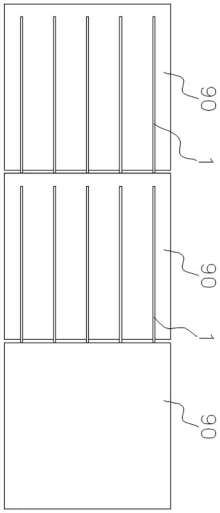
[0065] Figure 5 The connection state of the photovoltaic ribbon and the photovoltaic cell sheet 90 according to the first alternative embodiment is shown. Among them, the firs...
Embodiment approach 2
[0068] see Figure 6A-6C , which respectively show cross-sectional views of the first segment 101 , the second segment 103 and the third segment 104 of the photovoltaic ribbon according to the second alternative embodiment of the present invention.
[0069] Wherein, in the first segment body 101, a solder layer 12 is coated on the bottom surface, a black coating layer 13 is coated on other surfaces except the bottom surface, and a black coating layer 13 is coated on the entire surface of the second segment body 103. There is a black coating 13, and the third segment 104 has a coating structure symmetrical to that of the first segment, that is, a solder layer 12 is coated on the top surface, and a black coating is coated on other surfaces except the top surface. Layer 13.
[0070] Figure 7A with Figure 7B The connection states of the photovoltaic ribbons and the photovoltaic cells 90 according to the second alternative embodiment are shown respectively.
[0071] exist F...
PUM
 Abstract
Description
Claims
Application Information


