Microneedle electronic test system

An electronic testing and micro-needle technology, which is applied in electronic circuit testing, printed circuit testing, measuring electricity, etc., can solve the problems of single function of the testing system and low testing efficiency, and achieve the effect of improving the testing efficiency

Pending Publication Date: 2020-11-06
ZHUHAI BOJAY ELECTRONICS
View PDF0 Cites 0 Cited by
  • Summary
  • Abstract
  • Description
  • Claims
  • Application Information

AI Technical Summary

Problems solved by technology

However, the function of the existing test system is relatively single, and it can only perform one of the high-voltage and constant-current tests. Therefore, a PCB structure needs to perform multiple micro-needle contact tests in different test systems, resulting in low test efficiency.

Method used


Image

  • Microneedle electronic test system
  • Microneedle electronic test system
  • Microneedle electronic test system

Examples


Embodiment Construction

[0023] In order to enable those skilled in the art to better understand the solutions of the present invention, the following will clearly and completely describe the technical solutions in the embodiments of the present invention in conjunction with the drawings in the embodiments of the present invention. Obviously, the described embodiments are only It is an embodiment of a part of the present invention, but not all embodiments. Based on the embodiments of the present invention, all other embodiments obtained by persons of ordinary skill in the art without making creative efforts shall fall within the protection scope of the present invention.

[0024] It should be noted that the terms "first" and "second" in the description and claims of the present invention and the above drawings are used to distinguish similar objects, but not necessarily used to describe a specific sequence or sequence.

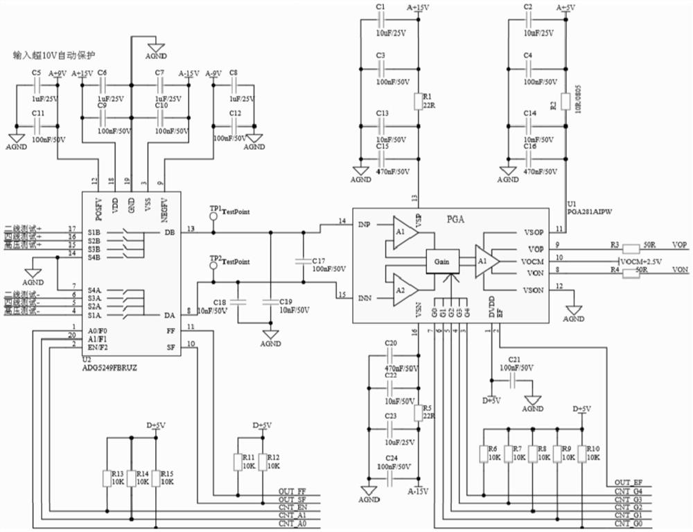
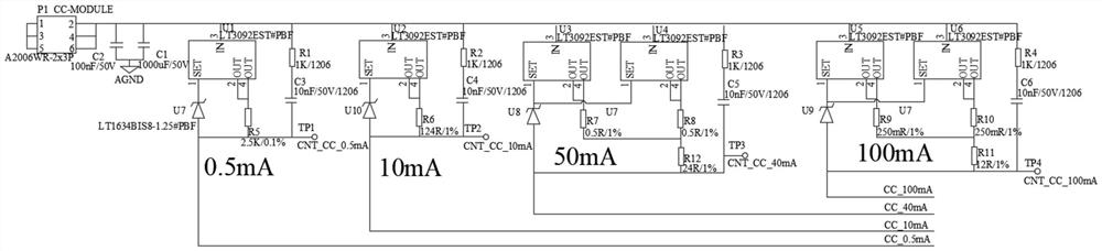
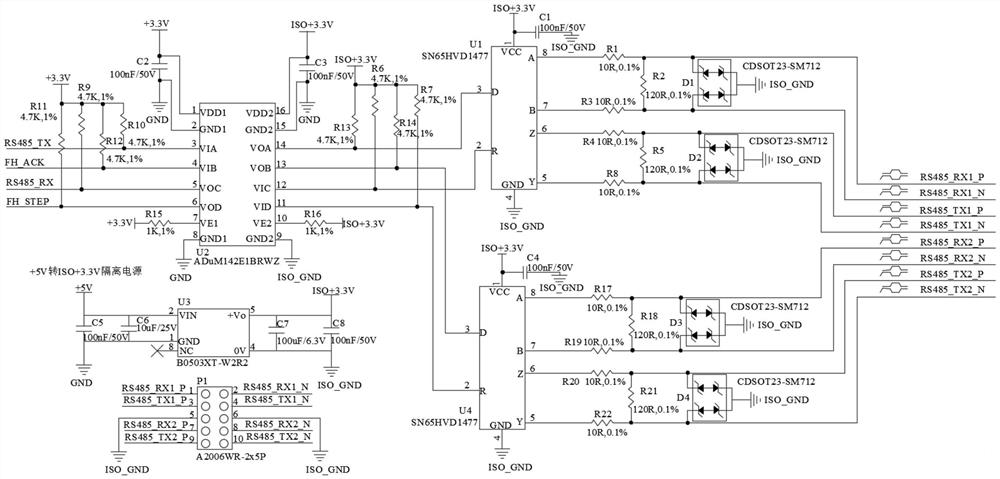
[0025] The embodiment of the present invention discloses a microneedle electronic...


PUM


Abstract

The invention provides a microneedle electronic test system, which comprises a control module, a signal acquisition module, a channel switching module, a communication control module and a microneedleelectronic test position, wherein the control module is electrically connected with the signal acquisition module; the signal acquisition module is electrically connected with the channel switching module; the control module is in communication connection with the channel switching module through the communication control module; the signal acquisition module is provided with a high-voltage source unit and a constant-current source unit; and the high-voltage source unit and the constant-current source unit are electrically connected with the microneedle electronic test position through the channel switching module. The microneedle electronic test system provided by the invention can be used for respectively carrying out high-voltage, constant-current and sampling tests in one connection test.

Description

technical field [0001] The invention relates to an electronic testing system, in particular to a microneedle electronic testing system. Background technique [0002] The Chinese name of PCB is printed circuit board, which is the carrier for the installation of electronic components and the basis for the electrical connection of electronic components. After the PCB is produced, high voltage, constant current and other tests are required to ensure that the product is qualified, so the electronic test system is used Use structures such as microneedles to contact PCB electronic components for detection. However, the function of the existing test system is relatively single, and it can only perform one of the high-voltage and constant-current tests. Therefore, a PCB structure needs to be tested for multiple micro-needle contacts in different test systems, resulting in low test efficiency. Contents of the invention [0003] The invention provides a microneedle electronic test s...

Claims


Application Information

Patent Timeline
Patent Type & Authority Applications(China)
IPC IPC(8): G01R31/28
CPCG01R31/2805G01R31/2806
Inventor 李志雄赵伟林梁树彬郑荣达蔡宇薛日胜杨进权周家进陈晓敏
Owner ZHUHAI BOJAY ELECTRONICS
Why Eureka
Try Eureka