Method for producing a single-crystal film of ALN material and substrate for the epitaxial growth of a single-crystal film of ALN mataleri

A technology of epitaxial growth and single crystal layer, which is applied in the directions of single crystal growth, single crystal growth, polycrystalline material growth, etc., and can solve the problem of not being able to obtain single crystal substrates

Pending Publication Date: 2020-11-06
SOITEC SA
View PDF7 Cites 0 Cited by
  • Summary
  • Abstract
  • Description
  • Claims
  • Application Information

AI Technical Summary

Problems solved by technology

[0002] Certain materials are not currently available as single crystal substrates in large diameter wafer form

Method used


Image

  • Method for producing a single-crystal film of ALN material and substrate for the epitaxial growth of a single-crystal film of ALN mataleri
  • Method for producing a single-crystal film of ALN material and substrate for the epitaxial growth of a single-crystal film of ALN mataleri
  • Method for producing a single-crystal film of ALN material and substrate for the epitaxial growth of a single-crystal film of ALN mataleri

Examples


Embodiment Construction

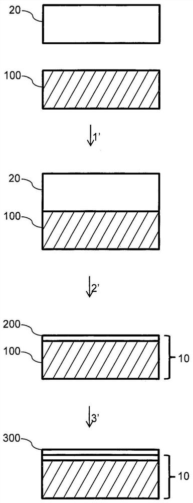
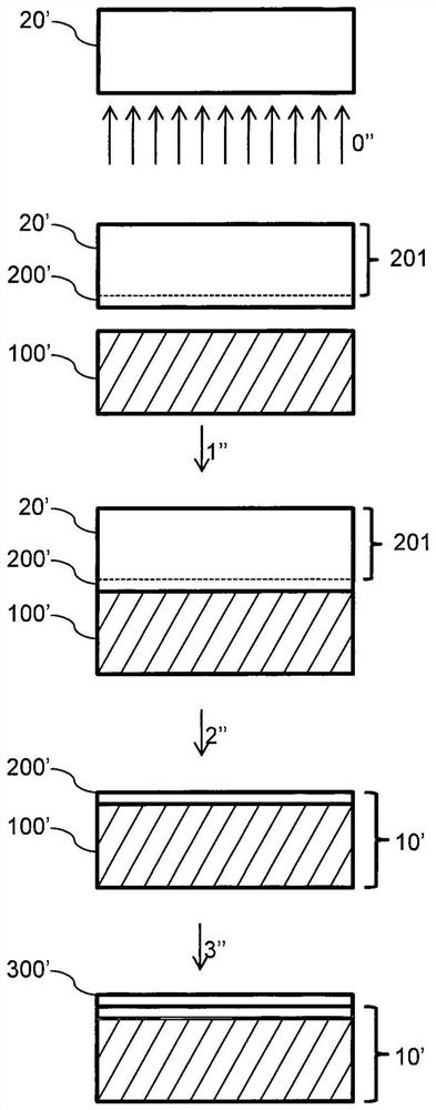
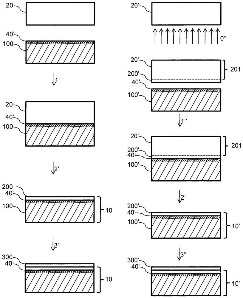
[0026] figure 1 A carrier substrate 100 of silicon material is shown, onto which a single crystal seed layer 200 of SiC-6H material is transferred. The carrier substrate 100 made of silicon material can also be replaced with the carrier substrate 100 made of sapphire material. The advantage of using silicon is that it not only opens up the application field of AlN material film for 300mm type large-scale equipment, but also makes it compatible with the microelectronics industry. For the microelectronics industry, foreign materials other than silicon, Especially AlN has high requirements in terms of acceptance. The step of bonding the single crystal seed layer 200 of SiC-6H material to the carrier substrate 100 of silicon material is preferably performed by a molecular adhesion step. The molecular adhesion step includes a bonding step, preferably performed at ambient temperature, followed by annealing to consolidate the bonding interface, which is usually performed at a high te...


PUM

PropertyMeasurementUnit
thicknessaaaaaaaaaa

Abstract

The invention relates to a method for producing a single-crystal film of AlN material, comprising the transfer of a single-crystal seed layer of SiC-6H onto a support substrate of silicon material, followed by the epitaxial growth of the single-crystal film of AlN material.

Description

Technical field [0001] The present invention relates to a method for producing a single crystal layer of aluminum nitride (AlN) material and a substrate for epitaxially growing the single crystal layer of this AlN material. Background technique [0002] Certain materials are currently not available as single crystal substrates in the form of large-diameter wafers. In addition, some materials are available in large diameters, but do not have certain characteristics or specifications in terms of quality, especially regarding defect density or required electrical or optical characteristics. Summary of the invention [0003] The purpose of the present invention is to overcome these limitations of the prior art by providing a method for manufacturing a single crystal layer of AlN material and a substrate for epitaxial growth of such a single crystal layer of AlN material. In this way, the size problem of the single crystal substrate of AlN material currently available can be solved. ...

Claims


Application Information

Patent Timeline
Patent Type & Authority Applications(China)
IPC IPC(8): C30B23/02C30B25/18C30B29/38C30B33/06H01L21/762
CPCC30B23/025C30B25/183C30B29/38C30B33/06H01L21/02658H01L21/02381H01L21/02447H01L21/0254C30B25/18C30B29/36C30B29/403H01L21/02488H01L21/02543H01L21/02546H01L21/02598
Inventor 布鲁诺·吉瑟兰
Owner SOITEC SA
Why Eureka
Try Eureka