Method for producing a monocrystalline layer of an LNO material and substrate for epitaxial growth of a monocrystalline layer of an LNO material

An epitaxial growth, single crystal layer technology, applied in the direction of single crystal growth, single crystal growth, polycrystalline material growth, etc., can solve the problem of not being able to obtain single crystal substrates

Pending Publication Date: 2020-11-06
SOITEC SA
View PDF3 Cites 0 Cited by
  • Summary
  • Abstract
  • Description
  • Claims
  • Application Information

AI Technical Summary

Problems solved by technology

[0002] Certain materials are not currently available as single crystal substrates in large diameter wafer form

Method used


Image

  • Method for producing a monocrystalline layer of an LNO material and substrate for epitaxial growth of a monocrystalline layer of an LNO material
  • Method for producing a monocrystalline layer of an LNO material and substrate for epitaxial growth of a monocrystalline layer of an LNO material
  • Method for producing a monocrystalline layer of an LNO material and substrate for epitaxial growth of a monocrystalline layer of an LNO material

Examples


Embodiment Construction

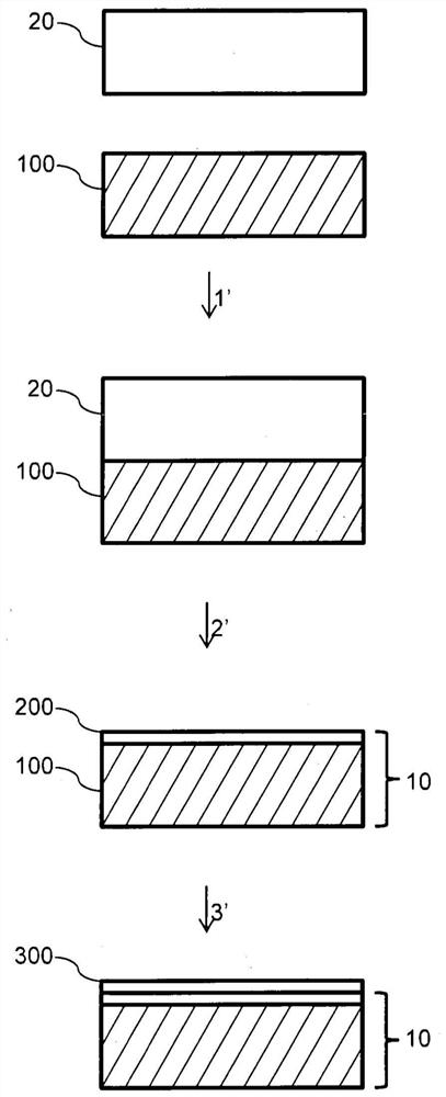
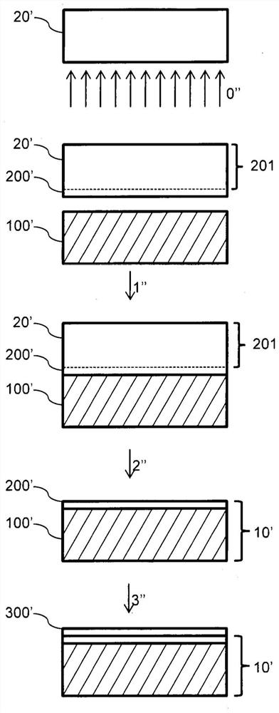
[0025] figure 1 A carrier substrate 100 of silicon material is shown, onto which a single crystal seed layer 200 of YSZ material is transferred. Other materials for the single crystal seed layer 200 are conceivable, such as SrTiO 3 , CeO 2 , MgO or Al 2 o 3 , these materials have lattice parameters close to those of LNO materials. The carrier substrate 100 of silicon material can also be replaced by a carrier substrate 100 of sapphire, Ni or Cu material. The advantage of using silicon is that it not only opens up the field of application of the LNO material layer for large devices of the 300mm type, but also makes it compatible with the microelectronics industry, for which there is no need for foreign materials other than silicon in the production line, In particular, LNO has high requirements in terms of acceptance. The step of bonding 1 ′ of the monocrystalline seed layer 200 of YSZ material to the carrier substrate 100 of silicon material is preferably performed by a ...


PUM

PropertyMeasurementUnit
thicknessaaaaaaaaaa

Abstract

The invention relates to a method for producing a monocrystalline layer of an LNO material, comprising the transfer of a monocrystalline seed layer of a YSZ material to a support substrate of a silicon material followed by epitaxial growth of the monocrystalline layer of LNO material.

Description

technical field [0001] The invention relates to a method for producing a single crystal layer of lithium niobate (LNO) material and a substrate for the epitaxial growth of such a single crystal layer of LNO material. Background technique [0002] Certain materials are not currently available as single crystal substrates in the form of large diameter wafers. Furthermore, certain materials are available in large diameters but do not have certain properties or specifications in terms of quality, especially with regard to defect density or desired electrical or optical properties. Contents of the invention [0003] The object of the present invention is to overcome these limitations of the prior art by providing a method for manufacturing a single crystal layer of LNO material and a substrate for epitaxial growth of such a single crystal layer of LNO material. In this way, the size problem of single crystal substrates of currently available LNO materials can be solved. [00...

Claims


Application Information

Patent Timeline
Patent Type & Authority Applications(China)
IPC IPC(8): C30B23/02C30B25/18C30B29/30C30B33/06H01L21/762
CPCH01L21/76254C30B23/025C30B25/183C30B29/30C30B33/06
Inventor 布鲁诺·吉瑟兰
Owner SOITEC SA
Why Eureka
Try Eureka