Microelement capable of being tested and micro-transferred, manufacturing, testing and transferring method of microelement and display device

A manufacturing method and technology for micro-components, which are applied in the fields of semiconductor/solid-state device testing/measurement, electrical components, semiconductor/solid-state device manufacturing, etc., can solve the problem of micro-components being unable to yield screening, and achieve improved light extraction efficiency and good current expansion. Effect

Pending Publication Date: 2020-11-13
XIAMEN QIANZHAO SEMICON TECH CO LTD
View PDF0 Cites 10 Cited by
  • Summary
  • Abstract
  • Description
  • Claims
  • Application Information

AI Technical Summary

Problems solved by technology

[0006] The purpose of the present invention is to provide a testable and micro-transferable micro-component and its production, testing and transfer method, and a display device to solve the problem in the prior art that micro-components cannot be electrically tested before transfer to achieve yield screening.

Method used


Image

  • Microelement capable of being tested and micro-transferred, manufacturing, testing and transferring method of microelement and display device
  • Microelement capable of being tested and micro-transferred, manufacturing, testing and transferring method of microelement and display device
  • Microelement capable of being tested and micro-transferred, manufacturing, testing and transferring method of microelement and display device

Examples


Embodiment 1

[0072] Such as figure 2 As shown, a micro-component that can be tested and micro-transferred, including:

[0073] supporting substrate 11;

[0074] A bonding layer 10, the bonding layer 10 is located on the surface of the supporting substrate 11;

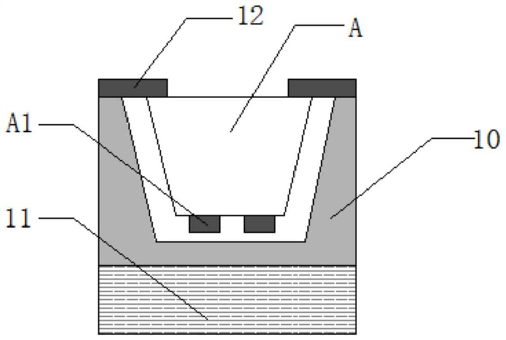
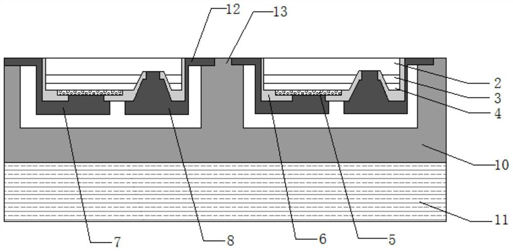
[0075] Light-emitting structure, the light-emitting structure includes several LED chips A that hang upside down on the support substrate 11 and are separated from each other by the groove A2, the bonding layer 10 is arranged on the surface of the support substrate 11 and embedded in the groove A2 to form a support column, and the key The composite layer 10 has an air gap with each LED chip A; each LED chip A includes an epitaxial layer, a protective layer 6 covering the exposed area of ​​the epitaxial layer, and a first electrode 7 and a second electrode located on the side of the epitaxial layer facing the supporting substrate 11. Electrode 8; the first electrode 7 and the second electrode 8 respectively extend to the surface o...

Embodiment 2

[0115] Such as figure 2 As shown, a micro-component that can be tested and micro-transferred, including:

[0116] supporting substrate 11;

[0117] A bonding layer 10, the bonding layer 10 is located on the surface of the supporting substrate 11;

[0118] Light-emitting structure, the light-emitting structure includes several LED chips A that hang upside down on the support substrate 11 and are separated from each other by the groove A2, the bonding layer 10 is arranged on the surface of the support substrate 11 and embedded in the groove A2 to form a support column, and the key The composite layer 10 has an air gap with each LED chip A; each LED chip A includes an epitaxial layer, a protective layer 6 covering the exposed area of ​​the epitaxial layer, and a first electrode 7 and a second electrode located on the side of the epitaxial layer facing the supporting substrate 11. Electrode 8; the first electrode 7 and the second electrode 8 respectively extend to the surface o...


PUM


Abstract

The invention provides a microelement capable of being tested and micro-transferred, a manufacturing, testing and transferring method of the microelement and a display device. A first electrode and asecond electrode of a LED chip extend to the surface of a bonding layer corresponding to a groove through the side wall of the LED chip respectively, so that the first electrode and the second electrode are exposed above the groove and play a role in supporting the LED chip in an inverted suspended state. And meanwhile, the first test electrode and the second test electrode can be used for carrying out an electrical test before the LED core particles are transferred, so that the yield screening of the LED core particles is realized, the LED core particles with abnormal electrical properties are prevented from being transferred to the substrate, and the repair cost is further reduced. And then, in a subsequent transfer process, metal of the first electrode and the second electrode exposed above the groove can be used as a chain for mass transfer, an exposed bonding layer is used as an anchor, and the micro-element is positioned to each anchor through transfer equipment, so that mass transfer of the micro-element can be realized.

Description

technical field [0001] The invention relates to the field of light-emitting diodes, in particular to a testable and micro-transferable micro-element, its manufacturing, testing and transfer methods, and a display device. Background technique [0002] Micro-component technology refers to an array of micro-sized components integrated at high density on a substrate. At present, micro-pitch light-emitting diode (Micro LED) technology has gradually become a research hotspot, and the industry expects high-quality micro-component products to enter the market. High-quality fine-pitch light-emitting diode products will have a profound impact on traditional display products such as LCD / OLED that are already on the market. [0003] In the process of fabricating microcomponents, the microcomponents are first formed on a donor substrate and then transferred to a receiving substrate. The receiving substrate is, for example, a display screen. One difficulty in the fabrication of microco...

Claims


Application Information

Patent Timeline
Patent Type & Authority Applications(China)
IPC IPC(8): H01L25/075H01L21/66H01L21/67H01L27/15
CPCH01L21/67144H01L22/30H01L25/0753H01L27/156
Inventor 江方吴双冯妍雪柯志杰艾国齐
Owner XIAMEN QIANZHAO SEMICON TECH CO LTD
Why Eureka
Try Eureka