Semiconductor LED structure with high extracting efficiency and its preparing method

A technology for light-emitting diodes and extraction efficiency, which is applied in semiconductor devices, electrical components, circuits, etc., and can solve problems such as low extraction efficiency, low external quantum efficiency, and low LED light intensity

Inactive Publication Date: 2008-03-12
BEIJING TIMESLED TECH CO LTD
View PDF2 Cites 0 Cited by
  • Summary
  • Abstract
  • Description
  • Claims
  • Application Information

AI Technical Summary

Problems solved by technology

A large amount of light is lost inside the LED, and only a small amount of light can be emitted to the outside, resulting in low external quantum efficiency of the LED. Low external quantum efficiency means low extraction efficiency and low light intensity of the LED.

Method used


Image

  • Semiconductor LED structure with high extracting efficiency and its preparing method
  • Semiconductor LED structure with high extracting efficiency and its preparing method

Examples


Embodiment

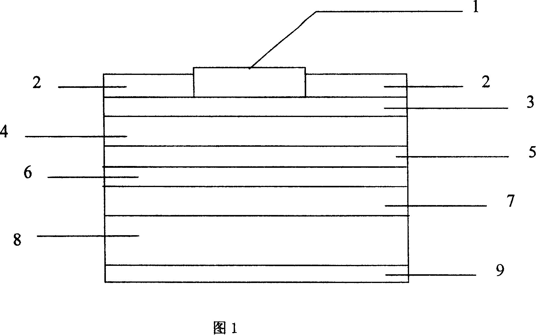
[0031] 1) Preparing a red LED epitaxial wafer, that is, growing an N-type semiconductor 7, a multi-quantum well active region 6, a P-type semiconductor 5, and a GaP layer 4 sequentially on a substrate 8, and the uppermost semiconductor material of the LED epitaxial wafer is GaP layer 4;

[0032] 2) Put the sample cleaned with acetone, absolute ethanol and deionized water into the ITO electron beam evaporation station, grow an ITO transparent conductive film 3 with an optical thickness of 1 / 2 wavelength on the GaP layer 4, and the growth temperature is 190 ℃, the oxygen flow rate is 3sccm, and the evaporation rate is 0.2nm / s; (In the actual preparation process, according to the conditions of your own equipment, you can flexibly adjust the growth process parameters such as growth temperature and oxygen flow rate to prepare the required ITO transparent conductive film3);

[0033] 3) Use PECVD equipment to grow Si on the ITO transparent conductive film 3 x N y Dielectric film 2...


PUM


Abstract

This invention puts forward that a compound reflection reducing coating composed of an ITO transparent conduction film and a SixNy medium film is grown on a LED epitaxial plate, in which, the optical thickness of the ITO transparent conduction film is the integral times of the half LED emission wavelength, the optical thickness of the SixNy medium film is the odd times of the quarter LED emission wave length, the refractive rate of the SixNy is the evolution of that of the top semiconductor material of the LED epitaxial plate, which can lower the interface reflection rate to the lowest to realize the best reflection reduction and increase foreign quanta effect.

Description

1. Technical field [0001] The invention belongs to the technical field of optoelectronic device manufacturing, and relates to a structure and a preparation method for improving the extraction efficiency of semiconductor light-emitting diodes (LEDs), which are suitable for semiconductor LEDs with various wavelengths (red light, blue light, green light, etc.). 2. Background technology [0002] Semiconductor light-emitting diodes are energy-saving, environmentally friendly and long-life light-emitting devices. LED energy consumption is 10% of incandescent lamps and 50% of fluorescent lamps. LED adopts solid packaging, firm structure, life span of 100,000 hours, 10 times that of fluorescent lamps and 100 times that of incandescent lamps. In terms of environmental protection, replacing incandescent or fluorescent lamps with LEDs does not require the use of glass vacuum packaging, and there is no pollution of toxic gas and mercury. And it has a wide range of uses, and can be app...

Claims


Application Information

Patent Timeline
Patent Type & Authority Patents(China)
IPC IPC(8): H01L33/00H01L33/38H01L33/44
Inventor 沈光地达小丽朱彦旭徐晨陈依新黄红娟
Owner BEIJING TIMESLED TECH CO LTD
Why Eureka
Try Eureka