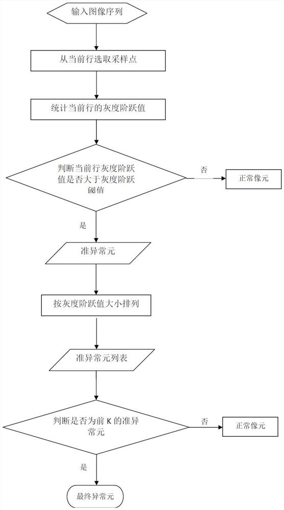
Abnormal element detection method for infrared array detector
A technology of infrared array and detection method, applied in instruments, image data processing, computing and other directions, can solve the problems of lack of real-time performance and low degree of automation, and achieve the effect of improving debugging efficiency and easy algorithm
- Summary
- Abstract
- Description
- Claims
- Application Information
AI Technical Summary
Problems solved by technology
Method used
Image
Examples
Embodiment Construction
[0015] In order to make the purpose, content, and advantages of the present invention clearer, the specific implementation manners of the present invention will be further described in detail below in conjunction with the accompanying drawings and embodiments.
[0016] The technical solution of the present invention: the infrared column detector realizes high-resolution imaging with a large field of view in a scanning manner, and each column (or row) of the image is obtained by imaging the same pixel. Using the imaging characteristics of the infrared line array detector and the neighborhood gray features of the abnormal elements and normal elements, mathematical statistics are carried out, and the position of the abnormal elements is judged according to the statistical results.
[0017] The example of the present invention takes the 576*4 long-wave infrared linear array detector as an example, assuming that the scanning direction is the row direction, and each row of the image ...
PUM
 Abstract
Description
Claims
Application Information
