Thin film transistor array substrate, pixel circuit, X-ray detector and driving method thereof

A technology of thin-film transistors and array substrates, which is applied in the field of pixel circuits, X-ray detectors and their drivers, and thin-film transistor array substrates. It can solve the problems of device output signal interference, large number of masks, and low refresh rate, etc., so as to improve the refresh rate. , Simplify the pixel structure and process structure, and reduce the effect of the use of photomasks

Active Publication Date: 2020-11-27
NANJING DETECH FUTURE TECH CO LTD
View PDF6 Cites 2 Cited by
  • Summary
  • Abstract
  • Description
  • Claims
  • Application Information

AI Technical Summary

Problems solved by technology

[0006] However, inside the pixel, due to the influence of the manufacturing process of the thin film transistor, the threshold voltage Vth of the thin film transistor will drift, which will cause certain interference to the output signal of the device
In addition, the existing detector manufacturing process also faces the problems of large number of masks, high cost and low refresh rate.

Method used


Image

  • Thin film transistor array substrate, pixel circuit, X-ray detector and driving method thereof
  • Thin film transistor array substrate, pixel circuit, X-ray detector and driving method thereof
  • Thin film transistor array substrate, pixel circuit, X-ray detector and driving method thereof

Examples


Embodiment Construction

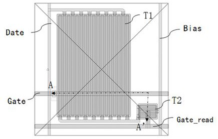
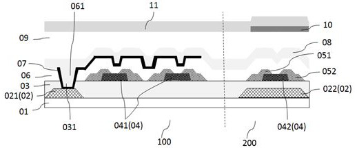
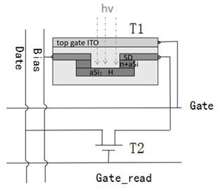
[0046] In order to more clearly illustrate the embodiments of the present invention or the technical solutions in the prior art, the specific implementation manners of the present invention will be described below with reference to the accompanying drawings. Obviously, the accompanying drawings in the following description are only some embodiments of the present invention, and those skilled in the art can obtain other accompanying drawings based on these drawings and obtain other implementations.

[0047] In order to make the drawing concise, each drawing only schematically shows the parts related to the present invention, and they do not represent the actual structure of the product. In addition, to make the drawings concise and easy to understand, in some drawings, only one of the components having the same structure or function is schematically shown, or only one of them is marked. Herein, "a" not only means "only one", but also means "more than one".

[0048] The techni...


PUM

PropertyMeasurementUnit
thicknessaaaaaaaaaa
thicknessaaaaaaaaaa
thicknessaaaaaaaaaa

Abstract

The invention provides a thin film transistor array substrate, a pixel circuit, an X-ray detector and a driving method thereof and relates to the technical field of photoelectricity. The thin film transistor array substrate comprises scanning lines, reading scanning lines, data lines and bias lines, wherein the scanning lines and the reading scanning lines are horizontally arranged, and the data lines and the bias lines are vertically arranged. The plurality of pixel units are defined by the scanning lines and the data lines in a crossed manner; each pixel unit comprises a photoconductive thinfilm transistor positioned in the photoconductive region and a reading thin film transistor positioned at the reading end. The photoconductive effect of the aSi thin film transistor is utilized to integrate the photocurrent and control the magnification times, so that the signal amplification in the pixel is realized, and the precise control of the magnification times can be realized while the radiation dose is reduced; meanwhile, the pixel structure and the process structure are simplified.

Description

technical field [0001] The invention belongs to the field of optoelectronic technology, and in particular relates to a thin film transistor array substrate, a pixel circuit, an X-ray detector and a driving method thereof. Background technique [0002] In recent years, radiographic imaging devices made of semiconductor materials to capture X-ray flat panel detectors have become more and more widely used in medical equipment, industrial non-destructive testing, and public safety. [0003] Flat-panel X-ray image detectors are generally classified into two thin film transistor array technologies. The first is an indirect detection image detector. For example, on the TFT pixel array made on the above substrate, a layer of photoelectric conversion film (such as hydrogenated amorphous silicon diode film) is deposited, and covered with a layer of material capable of converting X-rays into visible light, such as fluorescent film ( phosphors) or scintillation film (scintillattor), a...

Claims


Application Information

Patent Timeline
Patent Type & Authority Applications(China)
IPC IPC(8): H01L27/146H04N5/32G01T1/24
CPCG01T1/24G01T1/247H01L27/14612H01L27/14676H04N5/32
Inventor 陈钢
Owner NANJING DETECH FUTURE TECH CO LTD
Why Eureka
Try Eureka