Method and device for debugging plug-in chip through SDIO interface, equipment and medium

A technology of interface debugging and chips, which is applied in the computer field, can solve problems such as debugging inconvenience, and achieve the effect of convenient operation and cost saving

Active Publication Date: 2020-12-08
XIAMEN UNISOC TECH CO LTD
View PDF8 Cites 0 Cited by
  • Summary
  • Abstract
  • Description
  • Claims
  • Application Information

AI Technical Summary

Problems solved by technology

For example, when the external chip is an ARM chip, the ARM chip is integrated with the SWD debugging function, and the ARM core can be debugged through the SWD debugging interface during the development stage; Debugging is inconvenient

Method used


Image

  • Method and device for debugging plug-in chip through SDIO interface, equipment and medium
  • Method and device for debugging plug-in chip through SDIO interface, equipment and medium
  • Method and device for debugging plug-in chip through SDIO interface, equipment and medium

Examples


Embodiment 1

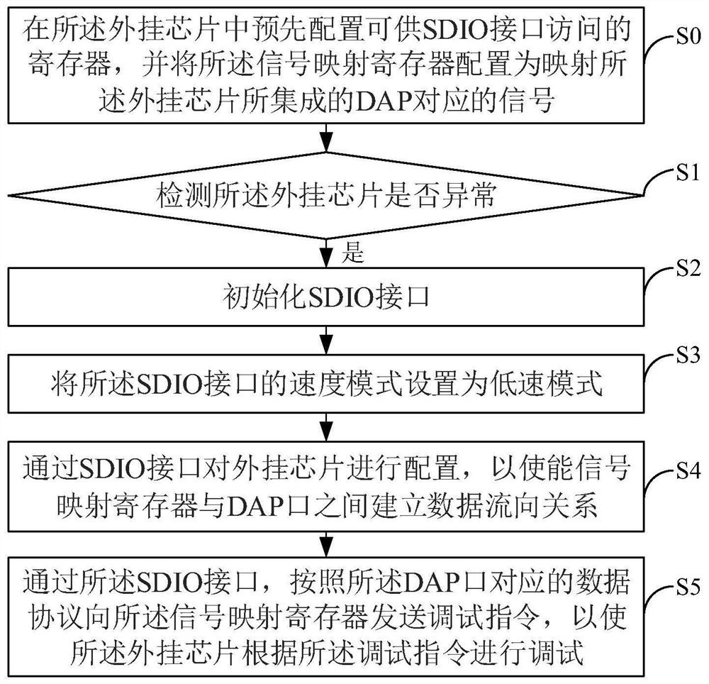
[0034] This embodiment provides a method for debugging a plug-in chip through an SDIO interface, which is suitable for a main control chip, and the main control chip communicates with the plug-in chip through an SDIO interface. like figure 1 As shown, the method includes the following steps:

[0035] S0, in the RFU (Reserved for Future Use, reserved for future use) subregion of the plug-in chip, pre-configure the registers (recorded as signal mapping registers) that can be accessed by the SDIO interface, and configure the signal mapping registers as Mapping the signals corresponding to the DAP integrated in the external chip.

[0036] In this embodiment, the external chip may be, for example, an ARM chip, and the ARM chip usually integrates a SWD interface as its DAP port. The SWD interface realizes the debugging of the ARM chip through a data line and a clock line, and its corresponding signals include data signals and clock signals.

[0037] On this basis, the signal mapp...

Embodiment 2

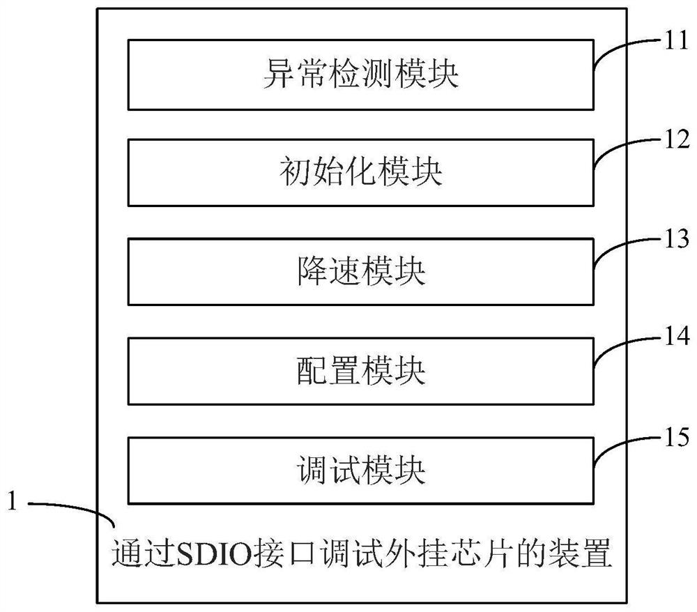
[0049] This embodiment provides a device for debugging a plug-in chip through an SDIO interface, which is suitable for a main control chip, and the main control chip communicates with the plug-in chip through an SDIO interface. Wherein, a register (referred to as a signal mapping register) accessible by the SDIO interface is pre-configured in the RFU partition of the external chip, and the signal mapping register is configured to map signals corresponding to the DAP integrated in the external chip.

[0050] In this embodiment, the external chip may be, for example, an ARM chip, and the ARM chip usually integrates a SWD interface as its DAP port. The SWD interface realizes the debugging of the ARM chip through a data line and a clock line, and its corresponding signals include data signals and clock signals.

[0051] On this basis, the signal mapping register is configured to map the data signal and clock signal of the DAP port. Specifically, four bits (bits) of the signal map...

Embodiment 3

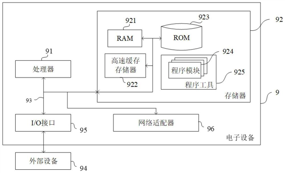
[0064] This embodiment provides an electronic device, which can be expressed in the form of a computing device (for example, it can be a server device), including a memory, a processor, and a computer program stored on the memory and operable on the processor, wherein the processor The steps of the method for debugging an external chip through the SDIO interface provided in Embodiment 1 can be implemented when the computer program is executed.

[0065] image 3 A schematic diagram of the hardware structure of this embodiment is shown, as image 3 As shown, the electronic device 9 specifically includes:

[0066] At least one processor 91, at least one memory 92, and a bus 93 for connecting different system components, including the processor 91 and the memory 92, wherein:

[0067] The bus 93 includes a data bus, an address bus, and a control bus.

[0068] The memory 92 includes a volatile memory, such as a random access memory (RAM) 921 and / or a cache memory 922 , and may fu...


PUM


Abstract

The invention provides a method and device for debugging a plug-in chip through an SDIO interface, equipment and a medium. A signal mapping register capable of being accessed by the SDIO interface isconfigured in the plug-in chip in advance, and the signal mapping register is configured to map a signal corresponding to a debugging access interface integrated by the plug-in chip. The method comprises the steps of initializing the SDIO interface; configuring the plug-in chip through the SDIO interface so as to enable a data flow direction relationship to be established between the signal mapping register and the debugging access interface; and sending a debugging instruction to the signal mapping register through the SDIO interface according to a data protocol corresponding to the debuggingaccess interface. The plug-in chip can be debugged through the SDIO interface so that a debugging interface does not need to be additionally led out, and a special debugging tool does not need to berelied on.

Description

technical field [0001] The invention relates to the technical field of computers, in particular to a method, device, equipment and medium for debugging an external chip through an SDIO interface. Background technique [0002] As the requirements for electronic products are getting higher and higher, relying on a single main control chip can no longer meet user needs. As a result, many plug-in chips that improve the work of auxiliary products have been derived. [0003] When the plug-in chip is abnormal, it needs to rely on a special debugging tool to debug it, so as to realize the fault location of the chip. On the one hand, this debugging solution increases the cost, and on the other hand, additional debugging interfaces need to be drawn out. [0004] After most products are mass-produced, the plug-in chip does not need to be debugged by default, so the debugging interface will not be led out. For example, when the external chip is an ARM chip, the ARM chip is integrated...

Claims


Application Information

Patent Timeline
IPC IPC(8): G06F11/26G06F11/263G06F11/273
CPCG06F11/261G06F11/263G06F11/273
Inventor 黄天宝
Owner XIAMEN UNISOC TECH CO LTD
Why Eureka
Try Eureka