Platform for detecting thickness of large-size wafer

A technology of wafer thickness and detection platform, applied in measurement devices, optical devices, mechanical measurement devices, etc., can solve problems such as inconvenience and high cleanliness requirements, cumbersome installation, etc., to ensure X-direction accuracy and movement speed. , the effect of simple maintenance, reducing the difficulty of processing and debugging

CN112129234APending Publication Date: 2020-12-25无锡星微科技有限公司
1 Cites 0 Cited by

Patent Information

Authority / Receiving Office
CN · China
Current Assignee / Owner
Publication Date
2020-12-25

Smart Images

  • Figure 1
    Figure 1
  • Figure 2
    Figure 2
  • Figure 3
    Figure 3
Patent Text Reader

Abstract

The invention provides a platform for detecting the thickness of a large-size wafer. The platform comprises a marble base, wherein a pair of Y-direction marble guide rail and Y-direction marble guiderail which are arranged in parallel are arranged on the marble base; a Y-direction sliding block and a Y-direction sliding block are arranged on the Y-direction marble guide rail and the Y-direction marble guide rail respectively; a Y-direction motor stator connecting piece and a Y-direction motor stator connecting piece are arranged on the outer side surface of each of the Y-direction marble guide rail and the Y-direction marble guide rail; a Y-direction grating reading device is arranged on each of the Y-direction sliding block and the Y-direction sliding block; and the Y-direction sliding block are connected through a Y-direction cross beam piece to form a Y-direction integral sliding block. According to the platform, an objective table adopts a hollow design, and a Y axis adopts a Y1 / Y2 bidirectional n-shaped air floatation double-drive design, so that the overall inherent frequency of the platform can be improved, the processing and debugging difficulty can be reduced, and the X-direction precision and the movement speed can be guaranteed; the jump of an object carrying surface is within 1 micron, so that the detection requirements of the industry that the size is increased day by day and is stricter day by day can be met; and an air floatation platform is simple to maintain, and a clean room is not polluted.
Need to check novelty before this filing date? Find Prior Art

Description

technical field

[0001] The invention mainly relates to the field of wafer detection, in particular to a large-size wafer thickness detection platform. Background technique

[0002] The existing motion platform used for the detection of wafer thickness and double-sided defects is a mechanical guide rail hollow platform. The platform is limited by the precision of the mechanical guide rail and the machining accuracy of the parts. The jump of the loading plane can only be a few microns larger, and the installation is cumbersome. , In addition, because the mechanical guide rail is a contact guide rail, it is easy to generate particles, which is inconvenient for occasions with high cleanliness requirements.

[0003] At present, the hollow air flotation platform used for the inspection of wafer thickness and double-sided defects, etc., due to the limitations of air flotation structure design, part processing accuracy and installation and debugging accuracy, the hollow diameter is ...

Examples

Embodiment Construction

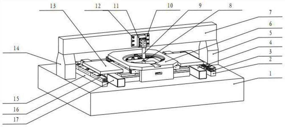
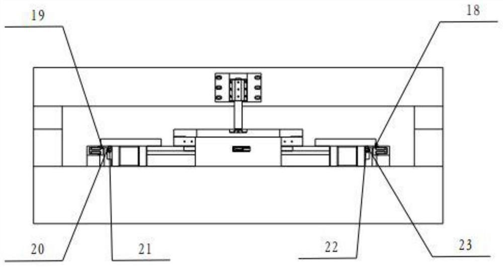
[0034] like Figure 1-5 It can be seen that the present invention includes: marble base (1), Y1 direction marble guide rail (4), Y2 direction marble guide rail (17), Y direction grating reading device and X direction grating reading device;

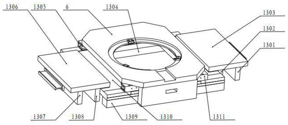
[0035] A pair of Y1 to marble guide rails (4) and Y2 to marble guide rails (17) arranged in parallel are installed on the marble base (1), and the Y1 to marble guide rails (4) and Y2 to marble guide rails (17) respectively A Y1-direction slider and a Y2-direction slider are provided, and a Y1-direction motor stator connector (2) and a Y2-direction motor stator connector (15) are provided on the outer surface, and the Y1-direction slider and the Y2-direction slider are both Equipped with a Y-direction grating reading device,

[0036] The Y1-direction slider and the Y2-direction slider are connected by a Y-direction beam (1310) to form a Y-direction overall slider, and the outer surfaces of the Y1-direction slider and the Y2-direction slid...