Photoelectric dynamic modulation system and method based on nanometer paper-cut meta-structure surface
A metasurface and dynamic modulation technology, applied in optics, optical components, nonlinear optics, etc., can solve the problems of high physical properties of substrate materials, difficulty in ensuring modulation accuracy, and unsuitability for integration, etc., to achieve easy integration , improve the space-bandwidth product, and achieve the effect of repeated changes
- Summary
- Abstract
- Description
- Claims
- Application Information
AI Technical Summary
Problems solved by technology
Method used
Image
Examples
Embodiment 1
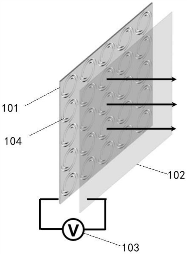
[0035] see figure 1 , which shows a photoelectric dynamic modulation system based on a nano-kirigami metasurface, the photoelectric dynamic modulation system based on a nano-kirigami metasurface 101 includes:
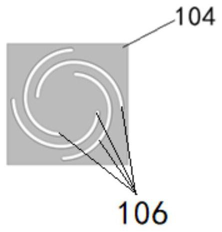
[0036] The nano-kirigami metasurface 101 includes a nano-conductive film and a nano-kirigami structural unit 104 arranged on the nano-conductive film;
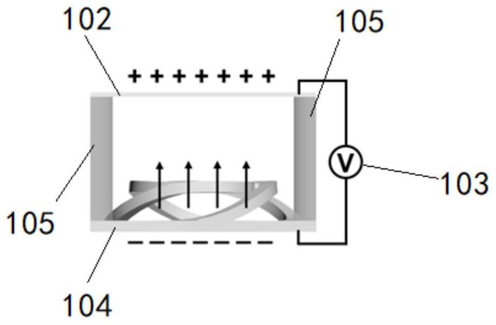
[0037] The voltage driving unit 103 is used to apply a voltage between the nano-kirigami structural unit 104 and the opposite transparent electrode 102 so that the nano-kirigami structural unit 104 produces three-dimensional elastic deformation; and
[0038] A voltage adjustment unit (not shown), used to adjust the voltage of the voltage driving unit 103 to realize dynamic modulation of the optical wavefront.
[0039] It can be understood that any nano-kirigami structural unit 104 with any structure capable of producing three-dimensional elastic deformation can be used in the present invention. The nano kirigami struc...
Embodiment approach
[0044] According to another preferred embodiment of the present invention, there is also provided a photoelectric dynamic modulation method based on the nano-kirigami metasurface 101, which is characterized in that it includes the following steps:
[0045]The nano kirigami structural unit 104 arranged on the nano conductive film;
[0046] A transparent electrode 102 is arranged opposite to the nano-kirigami structural unit 104, and a voltage is applied between the nano-kirigami structural unit 104 and the transparent electrode 102 so that the nano-kirigami structural unit 104 produces three-dimensional elastic deformation;
[0047] The voltage of the voltage driving unit 103 is adjusted to realize dynamic modulation of the optical wavefront.
[0048] According to yet another preferred embodiment of the present invention, an array of nano-kirigami structural units 104 is arranged on the nano-conductive film.
[0049] According to yet another preferred embodiment of the present...
PUM
 Abstract
Description
Claims
Application Information


