A kind of display circuit board and its manufacturing method, led display screen

A technology of LED display screen and display circuit, which is applied in the direction of circuits, electrical components, electric solid devices, etc. It can solve the problems of bulky structure and low pixels, achieve high circuit precision, solve current voltage drop and signal attenuation, and reduce drilling The effect of the amount

Active Publication Date: 2021-07-13
熊周成
View PDF10 Cites 0 Cited by
  • Summary
  • Abstract
  • Description
  • Claims
  • Application Information

AI Technical Summary

Problems solved by technology

[0005] In view of the above-mentioned shortcomings and deficiencies of the prior art, the present invention provides a display circuit board and its manufacturing method, and an LED display screen, which solves the problem that the prior art micro-pitch LED display screen is limited by the structure of the light board and has a bulky structure and low pixels. The problem

Method used


Image

  • A kind of display circuit board and its manufacturing method, led display screen
  • A kind of display circuit board and its manufacturing method, led display screen
  • A kind of display circuit board and its manufacturing method, led display screen

Examples


Embodiment 1

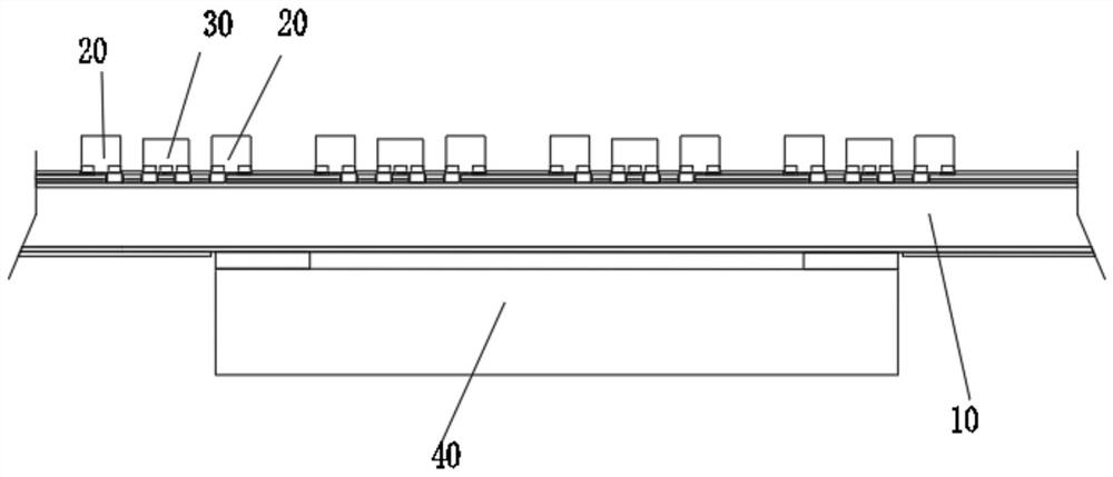
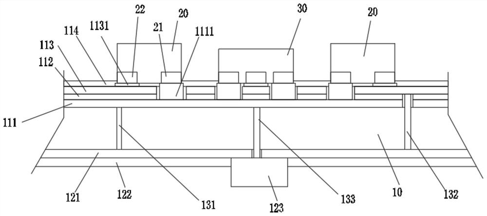
[0053] Embodiment 1 of the present invention provides a display circuit board. see Figure 1 to Figure 3 , the display circuit board includes a glass substrate 10 , a plurality of flip-chip bare-chip LED light-emitting chips 20 , a plurality of bare-chip constant current drive chips 30 and a control element 40 .

[0054]The glass substrate 10 can be a TFT glass substrate with a thickness of 0.3 mm to 2.0 mm, and its front is provided with a first circuit layer 111 , an intermediate insulating layer 112 , a second circuit layer 113 and a first surface insulating layer 114 in sequence. A third circuit layer 121 and a second surface insulating layer 122 are provided on the back of the glass substrate 10 .

[0055] In practical applications, the thickness of the insulating layer is about 0.1um-10um, and the thickness of the circuit layer is about 1um-35um.

[0056] The glass substrate 10 is also provided with a plurality of conductive holes (such as the first conductive hole 131...


PUM

PropertyMeasurementUnit
thicknessaaaaaaaaaa

Abstract

The invention discloses a display circuit board, a manufacturing method thereof and an LED display screen, belonging to the technical field of micro-pitch display screens. The circuit board includes a glass substrate and a plurality of electronic components arranged on the glass substrate; the front and back of the glass substrate are provided with circuit layers, and at least one of the circuit layers on the front or back is a multi-layer circuit layer, wherein the multiple Each circuit layer of the layer circuit layer is provided with an insulating layer, and the insulating layer is provided with a window to realize the electrical connection between the circuit layers and the electrical connection between the circuit layer and the electronic components; The flip-chip bare crystal LED light emitting chip and the bare crystal constant current driver chip on the front side of the substrate, wherein each bare crystal constant current driver chip drives at least one flip chip bare crystal LED light emitting chip. By adopting the present invention, the pixel pitch of the LED display screen can be effectively reduced, and the stability of the display image signal, the simplicity of product construction process integration and the seamless splicing among LED display units can be realized.

Description

technical field [0001] The invention relates to the technical field of LED display screens, in particular to a display circuit board, a manufacturing method thereof, and an LED display screen. Background technique [0002] With the development of LED display technology, micro-pitch LED (miniLED) display has gradually occupied an important position in the LED display technology industry due to its small spacing, clear display screen, and low power consumption. Most of the LED displays are spliced ​​by multiple display modules. Each display module includes a PCB board and at least one light board fixed on the PCB. The light board is equipped with multiple full-color RGB (red, yellow, blue) Three primary colors) LED lights, each light board is equipped with an external constant current drive circuit board, the constant current drive circuit board and each display module are connected to the HUB board through a transmission cable to realize receiving and transmitting control sig...

Claims


Application Information

Patent Timeline
Patent Type & Authority Patents(China)
IPC IPC(8): G09F9/33H01L25/16H01L25/00
CPCG09F9/33H01L25/167H01L25/50
Inventor 熊周成胡小龙叶裕清
Owner 熊周成
Why Eureka
Try Eureka