Programmable logic device grouping method and device

A programming logic and grouping method technology, which is applied in the field of programmable logic device grouping methods and devices, can solve problems such as unusable industrial design and circuit design failure, and achieve the effects of small division interconnection, fast speed, and improved processing efficiency

Active Publication Date: 2021-01-15
S2C
View PDF3 Cites 3 Cited by
  • Summary
  • Abstract
  • Description
  • Claims
  • Application Information

AI Technical Summary

Problems solved by technology

Under this constraint, it is easy to divide the program blocks connected by multiple virtual circuits in the logic circuit design, and divide them into FPGAs without physical circuit connections, which will lead to the failure of the circuit design. Such logic circuit design division is Invalid segmentation, cannot be used in industrial design

Method used


Image

  • Programmable logic device grouping method and device
  • Programmable logic device grouping method and device
  • Programmable logic device grouping method and device

Examples


Embodiment Construction

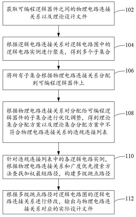
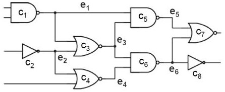
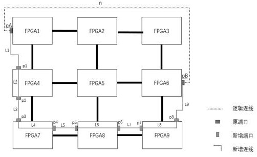
[0020] Embodiments of the present application will be described in detail below in conjunction with the accompanying drawings.

[0021] Embodiments of the present application are described below through specific examples, and those skilled in the art can easily understand other advantages and effects of the present application from the content disclosed in this specification. Apparently, the described embodiments are only some of the embodiments of this application, not all of them. The present application can also be implemented or applied through other different specific implementation modes, and various modifications or changes can be made to the details in this specification based on different viewpoints and applications without departing from the spirit of the present application. It should be noted that, in the case of no conflict, the following embodiments and features in the embodiments can be combined with each other. Based on the embodiments in this application, all...


PUM


Abstract

The invention provides a programmable logic device grouping method and device, belongs to the field of integrated circuit chip design, and particularly comprises the steps of obtaining a physical circuit connection relationship between programmable logic devices and a logic circuit diagram; clustering logic circuit instances in the logic circuit diagram to obtain a plurality of subsets; distributing all the subsets to a programmable logic device according to a physical circuit connection relationship; optimizing and adjusting the subset allocated to the programmable logic device to obtain a theoretical set allocation scheme and an illegal connection list; constructing a multi-level jump point path for each logic circuit instance in the violation connection list; and modifying the logic circuit connection relationship according to the multi-stage jump point path, and outputting an actual design file corresponding to the physical circuit connection relationship. By means of the processing scheme, the programmable logic device grouping result which is minimum in segmentation interconnection, higher in speed and larger in data processing scale is obtained, and therefore the chip processing efficiency is improved.

Description

technical field [0001] The invention relates to the field of integrated circuit chip design, in particular to a programmable logic device grouping method and device. Background technique [0002] EDA technology is based on large-scale programmable devices, using computers as tools, completing expressions according to the hardware description language HDL, and realizing the goals of logic compilation, simplification, segmentation, layout, and optimization. With the help of EDA technology, the operator The description of hardware functions can be realized by using software, and the final design result can be obtained through FPGA / CPLD. Existing very large scale integration (VLSI: Very Large Scale Integration) refers to an integrated circuit with tens of thousands to millions of transistors integrated on a silicon chip of a few millimeters square, and a line width of less than 1 micron. Therefore, the complexity of VLSI circuits is a challenge for EDA design. Circuit segmenta...

Claims


Application Information

Patent Timeline
Patent Type & Authority Applications(China)
IPC IPC(8): G06F30/367
CPCG06F30/367
Inventor 李伟张吉锋林铠鹏邵中尉
Owner S2C
Why Eureka
Try Eureka