Semiconductor laser coherent array and preparation method thereof

A laser and semiconductor technology, applied in semiconductor lasers, semiconductor laser devices, lasers, etc., can solve the problems of low heat dissipation performance of devices, low power amplifier effect, low optical efficiency, etc., to improve quality, reduce heat consumption, and avoid phase mismatch. Effect

Active Publication Date: 2021-01-19
INST OF SEMICONDUCTORS - CHINESE ACAD OF SCI
View PDF5 Cites 2 Cited by
  • Summary
  • Abstract
  • Description
  • Claims
  • Application Information

AI Technical Summary

Problems solved by technology

[0003]Currently, the coherent technologies of array lasers mainly include evanescent wave coupling, Y-shaped waveguide array and Talbot coupling cavity structure, etc. The waveguide array and the Talbot coupling cavity structure are respectively limited by maintaining a specific finite distance, poor heat dissipation of the device, and difficulty in maintaining a continuous operating wave mode, etc., which have low output power amplifier effect, low optical efficiency, and low heat dissipation performance of the device. and other defects

Method used


Image

  • Semiconductor laser coherent array and preparation method thereof
  • Semiconductor laser coherent array and preparation method thereof
  • Semiconductor laser coherent array and preparation method thereof

Examples


Embodiment Construction

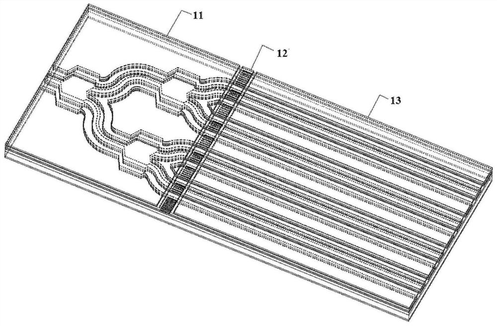
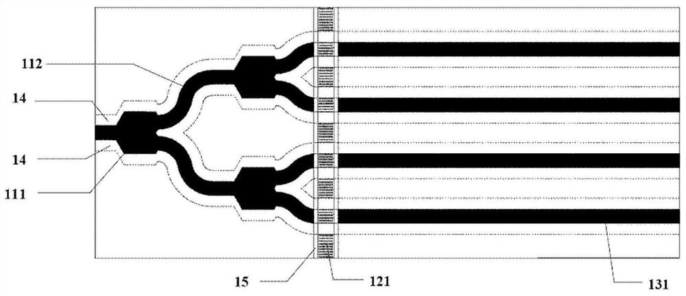
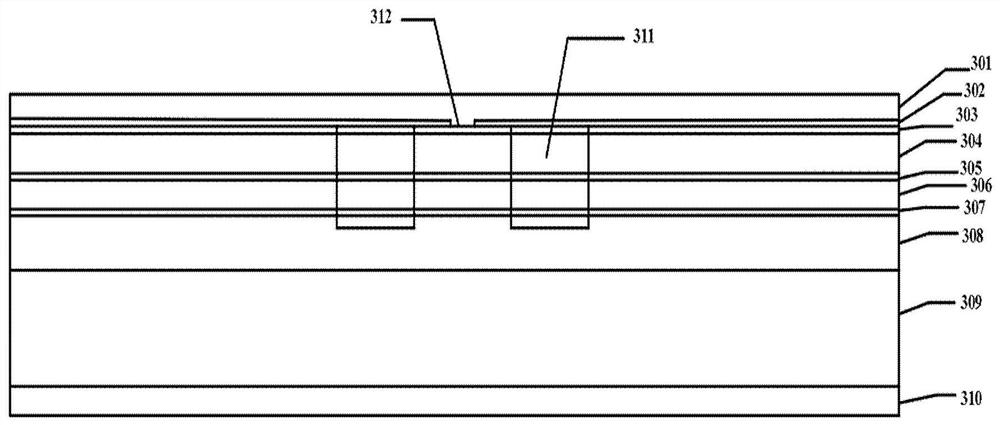
[0032] Hereinafter, embodiments of the present disclosure will be described with reference to the drawings. It should be understood, however, that these descriptions are exemplary only, and are not intended to limit the scope of the present disclosure. In the following detailed description, for purposes of explanation, numerous specific details are set forth in order to provide a thorough understanding of the embodiments of the present disclosure. It may be evident, however, that one or more embodiments may be practiced without these specific details. Also, in the following description, descriptions of well-known structures and techniques are omitted to avoid unnecessarily obscuring the concept of the present disclosure.

[0033] The terminology used herein is for the purpose of describing particular embodiments only, and is not intended to be limiting of the present disclosure. The terms "comprising", "comprising", etc. used herein indicate the presence of stated features, ...


PUM

PropertyMeasurementUnit
widthaaaaaaaaaa
lengthaaaaaaaaaa
radiusaaaaaaaaaa

Abstract

The invention provides a semiconductor laser coherent array, and the array is characterized in that the semiconductor laser coherent array comprises a multi-mode interference region which comprises amulti-stage one-to-two multi-mode interference coupling structure and a plurality of bent waveguides, wherein the multi-mode interference coupling structure between different stages is connected through the bent waveguides, and the multi-stage one-to-two multimode interference coupling structure is used for generating a plurality of phase coherent optical branches; a reflection region which is used for transmitting the plurality of optical branches and controlling the energy ratio output by the optical branches by adjusting the reflectivity; and an array region which comprises a plurality of channel waveguides and is used for carrying out power amplification on the plurality of optical branches output by the reflection region and then outputting the amplified optical branches. The invention further provides a preparation method of the semiconductor laser coherent array.

Description

technical field [0001] The present disclosure relates to the field of semiconductor optoelectronic technology, in particular to a coherent array of semiconductor lasers and a preparation method thereof. Background technique [0002] Semiconductor lasers have the advantages of small size, high efficiency, and easy operation. However, due to the limited power of a single laser, it still cannot meet the needs in some application scenarios. The emergence of coherent array lasers enables semiconductor lasers to retain their advantages while having greater output power, which enriches the applications of photoelectric countermeasures, medical treatment, and information processing. Coherent array lasers use optical waveguide theory and technology to integrate multiple lasers into a single chip, so that effective coupling between each laser can be achieved to achieve coherent high-power output. The coherent array enables high output power while ensuring good output characteristics ...

Claims


Application Information

Patent Timeline
Patent Type & Authority Applications(China)
IPC IPC(8): H01S5/40H01S5/065H01S5/20
CPCH01S5/4006H01S5/4025H01S5/0653H01S5/20
Inventor 顾增辉张锦川刘峰奇
Owner INST OF SEMICONDUCTORS - CHINESE ACAD OF SCI
Why Eureka
Try Eureka