Optical neural network device, chip and optical implementation method for neural network calculation

A neural network and optical technology, applied in the field of photonic integration and high-performance computing, can solve the problems of high power consumption and cost of optical chips

Active Publication Date: 2021-02-02
WUHAN OPTICAL VALLEY INFORMATION OPTOELECTRONICS INNOVATION CENT CO LTD
View PDF4 Cites 3 Cited by
  • Summary
  • Abstract
  • Description
  • Claims
  • Application Information

AI Technical Summary

Problems solved by technology

However, too many modulators lead to high powe

Method used


Image

  • Optical neural network device, chip and optical implementation method for neural network calculation
  • Optical neural network device, chip and optical implementation method for neural network calculation
  • Optical neural network device, chip and optical implementation method for neural network calculation

Examples


Embodiment Construction

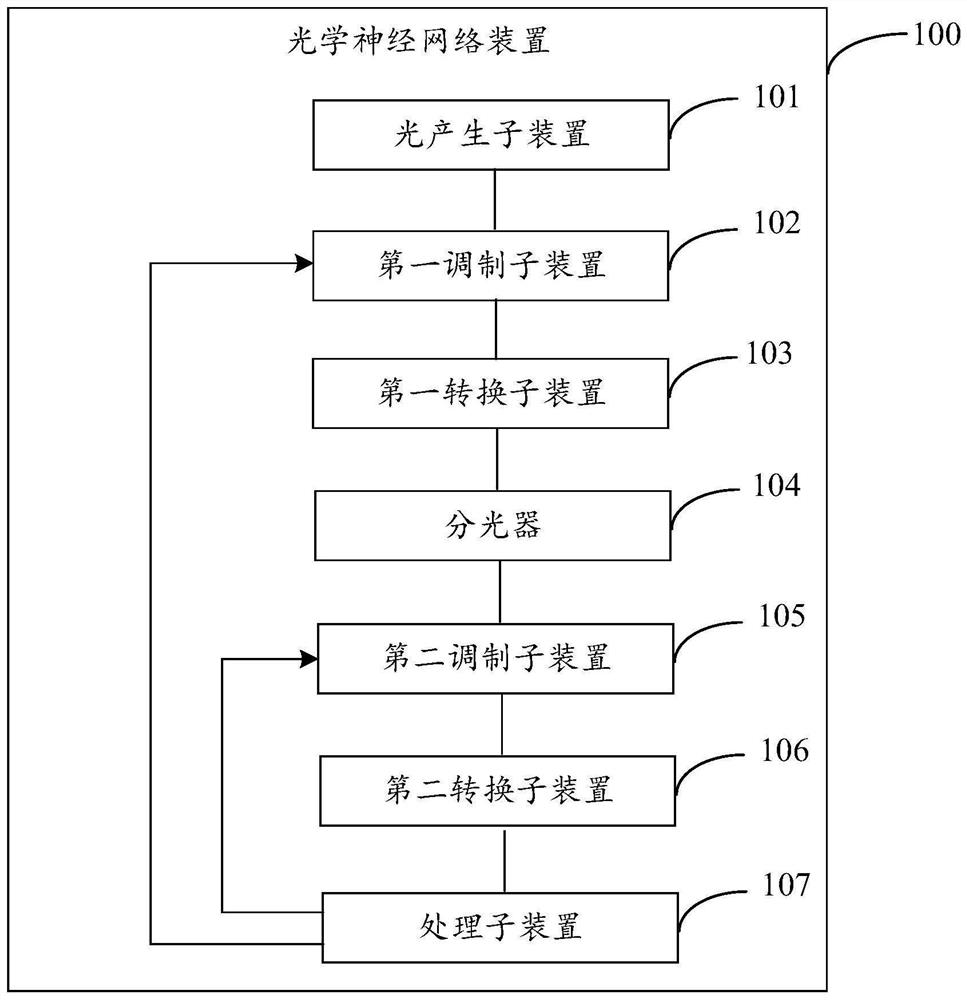
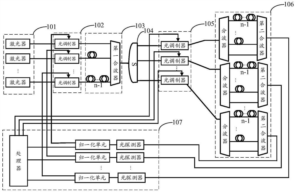
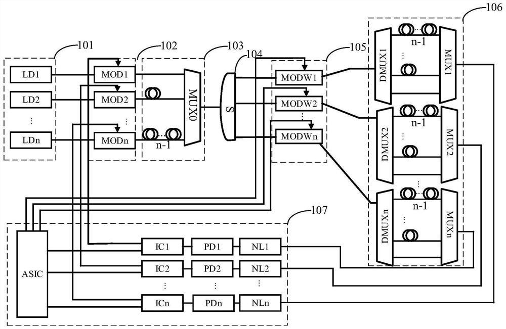
[0052] In order to make the technical solutions and advantages of the embodiments of the present invention more clear, the specific technical solutions of the invention will be further described in detail below in conjunction with the drawings in the embodiments of the present invention. The following examples are used to illustrate the present invention, but are not intended to limit the scope of the present invention.

[0053] In various embodiments of the embodiments of the present invention, the adjustment of the N first voltages is used to adjust the input value of each neural network layer in the neural network, and the adjustment of the N first voltage sets is used to realize the adjustment of the input value of each neural network layer in the neural network. Adjustment of the weight value. Since in the embodiment of the present invention, the input values ​​of each neural network layer are converted from parallel to serial, a sequence of optical signals is obtained, and...


PUM


Abstract

The embodiment of the invention provides an optical neural network device, a chip and an optical implementation method for neural network calculation. The device comprises: a light generation sub-device which is used for generating N paths of optical signals with different wavelengths, wherein the N is an integer greater than 1; a first modulation sub-device which is used for modulating the intensity of the N paths of optical signals according to the N first voltages to obtain N paths of first optical signals; a first conversion sub-device which is used for carrying out parallel-serial conversion on the N paths of first optical signals to obtain a second optical signal; an optical splitter which is used for splitting the second optical signal into N paths of third optical signals; a secondmodulation sub-device which is used for separately modulating the intensity of the N paths of third optical signals according to the N first voltage sets to obtain N paths of fourth optical signals;a second conversion sub-device which is used for performing serial-parallel conversion on each of the N paths of fourth optical signals to obtain N paths of fifth optical signals; and a processing sub-device which is used for adjusting the values of the N first voltages and the N first voltage sets based on the N paths of fifth optical signals.

Description

technical field [0001] The invention relates to the technical field of photon integration and high-performance computing, in particular to an optical neural network device, a chip and an optical realization method of neural network computing. Background technique [0002] Neural network calculation is one of the main functions of artificial intelligence chips. Neural network calculation needs to quickly complete a series of complex matrix multiplication operations. Neural network computing can be implemented using electrical chips. However, traditional electrical chips have limited computational efficiency due to the influence of process nodes and material properties. Photonic integrated devices, especially silicon-based photonic integrated devices, have developed rapidly in recent years. Silicon-based photonic integrated devices have the advantages of high speed, strong anti-interference ability, high integration, and semiconductor process compatibility. Beam splitting an...

Claims


Application Information

Patent Timeline
IPC IPC(8): G06N3/067G06N3/04G06N3/08
CPCG06N3/0675G06N3/08G06N3/045Y02D10/00
Inventor 王磊肖希李维忠胡晓李淼峰陈代高
Owner WUHAN OPTICAL VALLEY INFORMATION OPTOELECTRONICS INNOVATION CENT CO LTD
Why Eureka
Try Eureka