Display device and display device preparation method

A display device and display panel technology, which is applied in the direction of identification devices, instruments, etc., can solve the problems of poor image quality and large seams of display panels

Pending Publication Date: 2021-02-02
HISENSE VISUAL TECH CO LTD
View PDF0 Cites 3 Cited by
  • Summary
  • Abstract
  • Description
  • Claims
  • Application Information

AI Technical Summary

Problems solved by technology

[0004] The present invention provides a display device and a preparation method of the display device, which are used to solve the problems in the prior...

Method used


Image

  • Display device and display device preparation method
  • Display device and display device preparation method
  • Display device and display device preparation method

Examples


Embodiment Construction

[0035] The application scenarios described in the embodiments of the present invention are to illustrate the technical solutions of the embodiments of the present invention more clearly, and do not constitute limitations on the technical solutions provided by the embodiments of the present invention. It appears that the technical solutions provided by the embodiments of the present invention are also applicable to similar technical problems. Wherein, in the description of the present invention, unless otherwise specified, "plurality" means two or more.

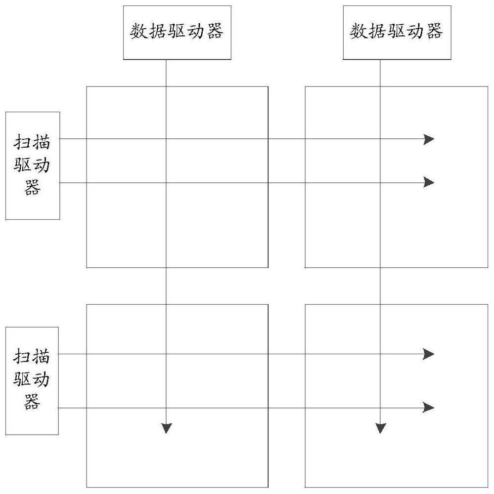
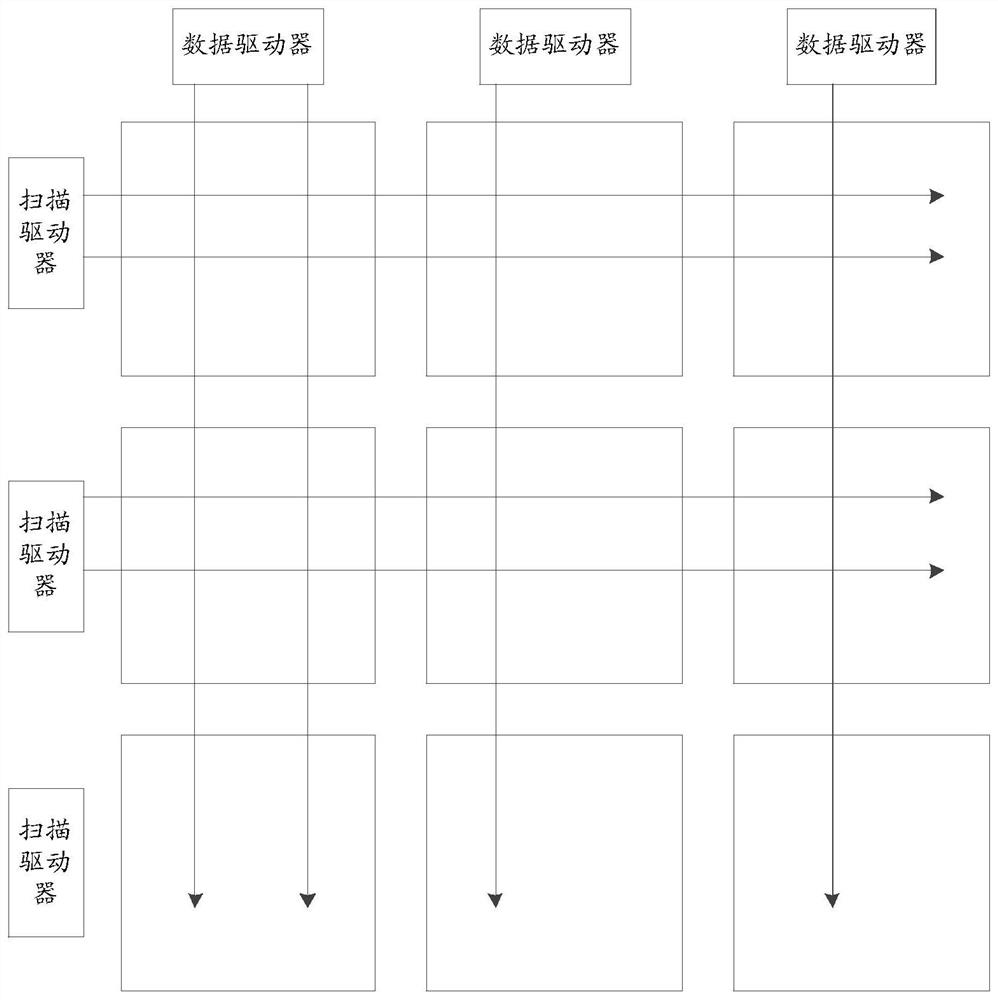
[0036] In the display device based on the TFT LED display panel, the display panel is formed by splicing multiple panels, such as Figure 1A and Figure 1B As shown, it is the arrangement of the two panels in the prior art when they are spliced ​​together. At the same time, one or both sides of the panel are provided with built-in data lines and scanning drive circuits, and are connected through external pins; because the two ...


PUM


Abstract

The invention provides a display device and a preparation method of the display device which are used for solving the problems of large splicing seams and poor image quality of a display panel due tothe fact that an micro LED is electrically connected through an external driver. The device comprises a display panel and a flexible substrate located on the side, deviating from a light emitting surface, of the display panel. The surface, facing the display panel, of the flexible substrate is provided with a conductive structure. A signal line and/or a data line are/is arranged on one side, deviating from the flexible substrate, of the display panel; the display panel comprises a plurality of sub-panels distributed in an array mode, in every two adjacent sub-panels in the row direction and/orthe column direction, the edge, adjacent to the other sub-panel, of one sub-panel is provided with a plurality of conductive channels, the conductive channels are filled with electric conductors, oneend of each electric conductor is connected with a conductive structure, and the other end of each electric conductor is connected with the signal line and/or the data line. the sub-panels are not electrically connected through the external driver, and a plurality of scanning and data circuits are arranged, so that the image quality of the display panel is improved.

Description

technical field [0001] The invention relates to the field of display technology, in particular to a display device and a method for manufacturing the display device. Background technique [0002] Micro LED (micron-scale light-emitting diode) is considered to be an ideal form of future display technology because of its high brightness, fast response, and high stability. At present, the display of Micro LED only has small-sized panels, based on CMOS (Complementary Metal Oxide Semiconductor, Complementary Metal Oxide Semiconductor), PCB (Printed Circuit Board, Printed Circuit Board) or TFT (Thin Film Transistor, Thin Film Transistor), large size based on PCB display can be realized by splicing, but the resolution is low. In order to realize high-resolution Micro LED display, TFT driving technology is necessary. [0003] At present, the panel displayed by TFT-based LED (Light Emitting Diode, light-emitting diode) is smaller than 5 inches, and multiple panels need to be spliced....

Claims


Application Information

Patent Timeline
IPC IPC(8): G09F9/33G09F9/302
CPCG09F9/3026G09F9/33
Inventor 李潇金南德
Owner HISENSE VISUAL TECH CO LTD
Why Eureka
Try Eureka